
November 4, 2014
November 1, 2014
BFR93 - BJT RF transistor : weekend die-shot
BFR93 is a popular, BJT npn RF transistor.Die size 265x264 µm. Transistor itself occupy only small part of the die - it is impractical to cut smaller die, it is already almost a silicon cube:


October 27, 2014
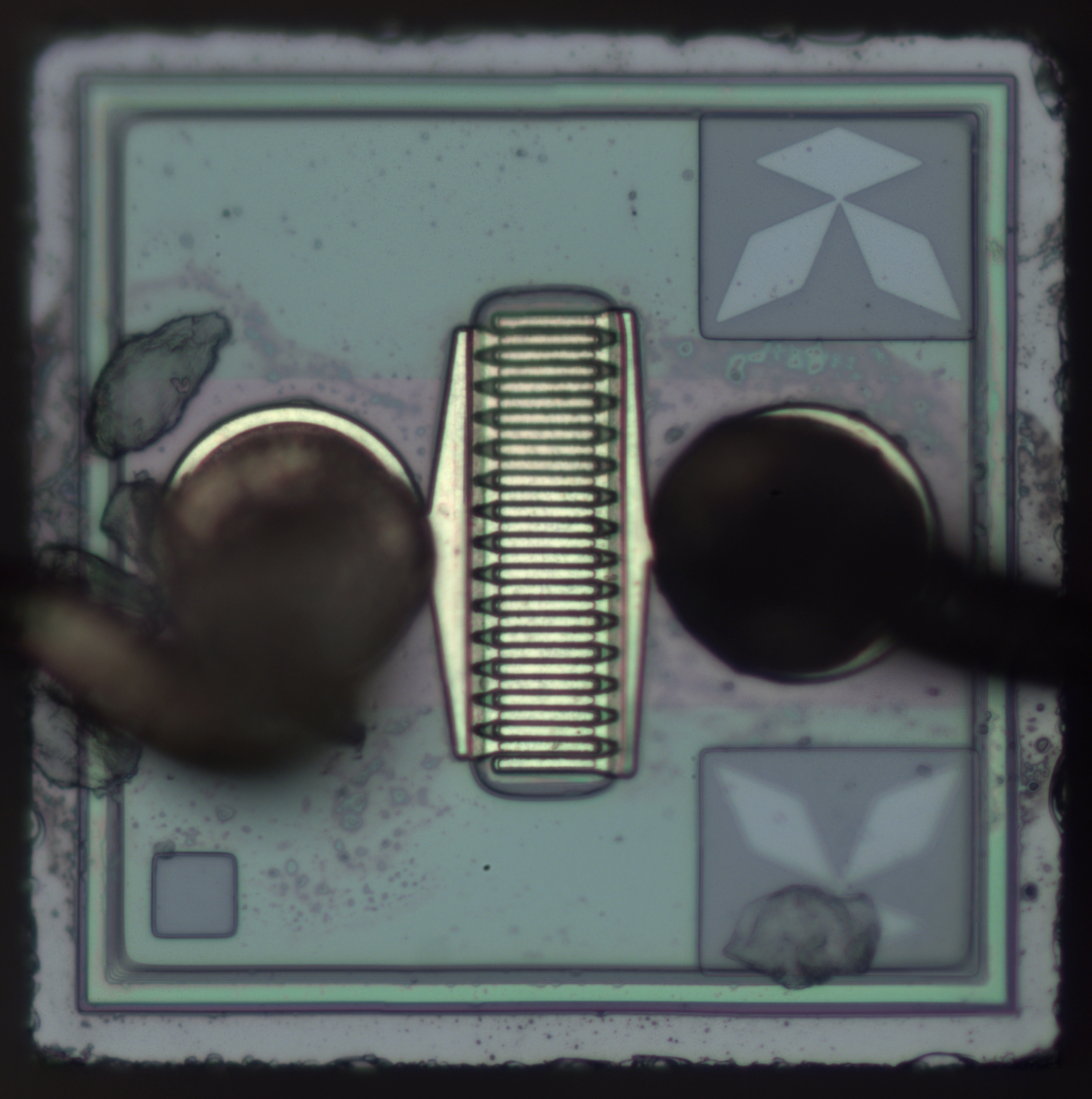
10Mhz Quartz SMD oscillator based on Seiko NPC SM5009 : weekend die-shot
Seiko NPC SM5009 contains internal load capacitors, oscillator with amplitude limiting (for reduced power consumption) and optional frequency divider.Die size 1194x897 µm, 800nm technology.

October 20, 2014
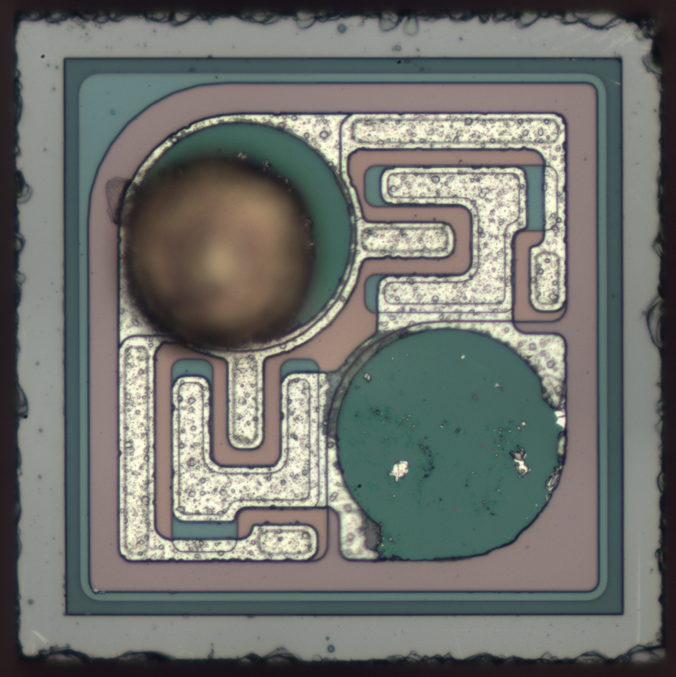
OnSemi MMBT2222A - npn BJT transistor : weekend die-shot
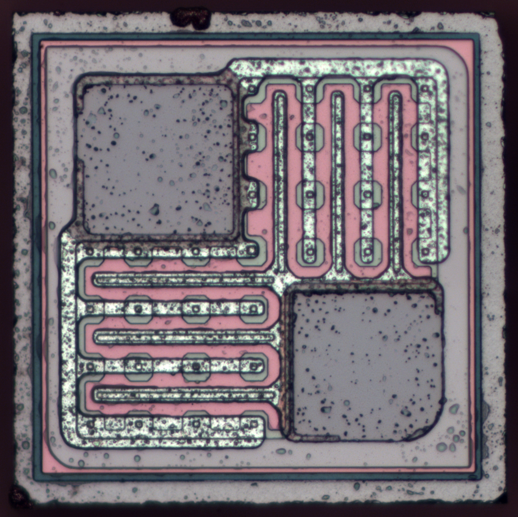
Die size 343x343 µm. Comparing to NXP BC847B die area is 1.5x larger (0.118 vs 0.076mm²), but maximum continuous collector current is 6 times higher (600mA vs 100mA, SOT-23 in both cases). This huge increase in current per transistor area is achieved by shunting thin (=high-resistance) base layer with metal. High resistance of base layer is the limiting factor for maximum collector current in BC847B.
October 20, 2014
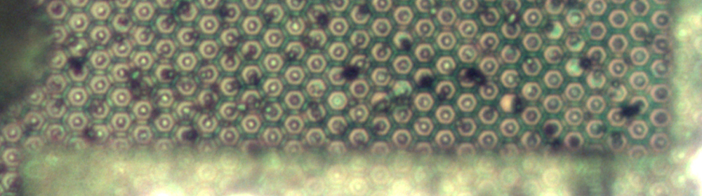
NXP 2N7002 N-channel MOSFET : weekend die-shot
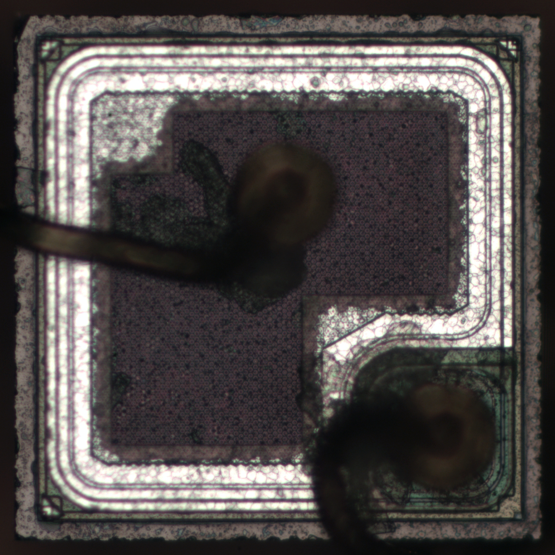
Die size 377x377 µm.
Hexagonal cells of TrenchMOS transistor has 4µm size.
October 20, 2014
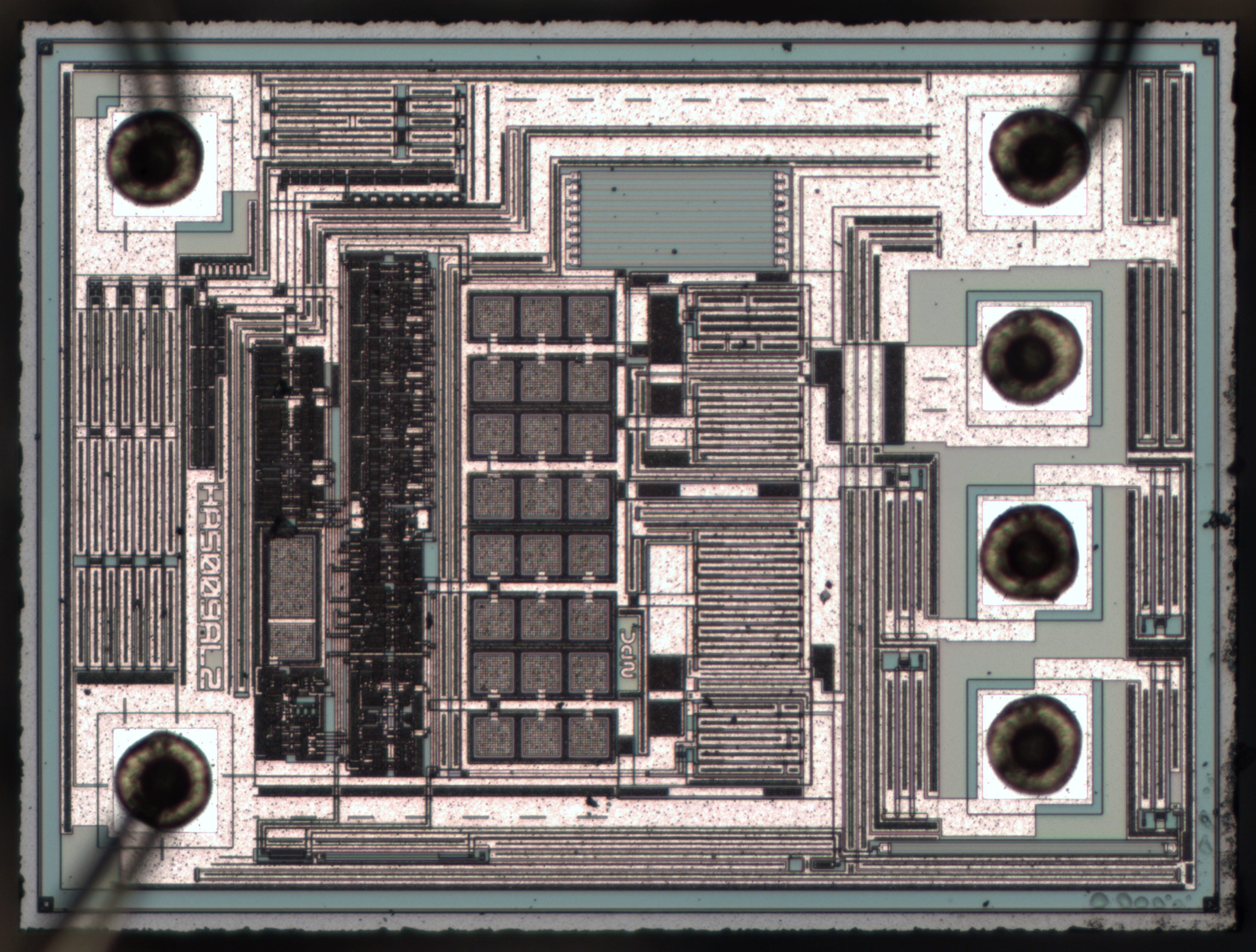
Espressif ESP8266 WiFi-serial interface : weekend die-shot
Since August of 2014 internet is literally blown by WiFi-serial modules on new ESP8266 chip which are currently being sold for less than 4$. Chinese company Espressif managed to cram entire WiFi, TCP/IP and HTTP stack into on-chip memory, without external DRAM. Analog front-end requires minimal external components, all filters are internal. All this allowed them to offer extremely aggressive price. Chip has marking ESP8089, which is their more advanced 40nm product. Apparently, they only differ in bonding and ROM content.Die size 2050x2169 µm, half of which is occupied by transceiver and PA, 25% - on-chip memory (rough size estimations are ~300KiB), and the rest is Xtensa LX106 CPU core and other digital logic.
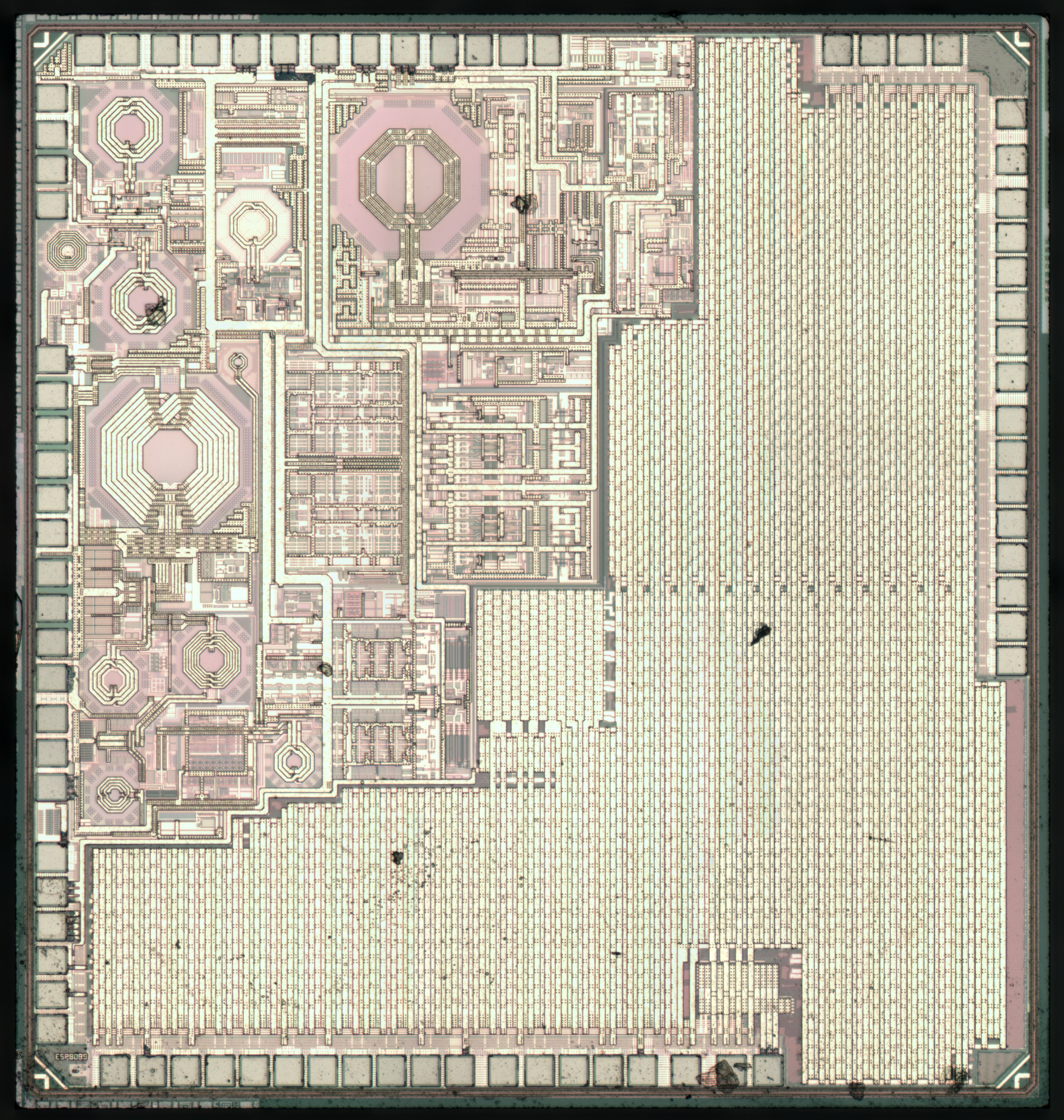
Chinese engineers did an outstanding job here on finally making WiFi IoT devices cost effective. Let's hope Espressif will eventually open more internal chip information for amateurs and end users.
October 7, 2014
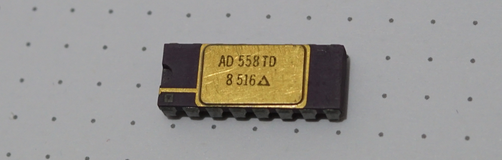
Analog Devices AD558 - MIL-Spec 8-bit I²L DAC : weekend die-shot
Analog Devices AD558 is an 8-bit I²L DAC in ceramic package (MIL spec).It is still an open question how this chip got into ex-USSR/Russia - anonymous reader left no comments on that (this smells like cold war...). It is not a secret that Russia had no extensive civilian IC assortment in manufacturing, hence all military IC's must have been designed and manufactured from scratch (i.e. all R&D, prototypes and masks must be paid by government). In such conditions providing all variety of domestic ICs is economically impossible, at least without government expenses comparable to whole world's expenses on IC R&D. So "temporary", "case-by-case" permit to use imported (both legitimately and not-so-legitimately) western ICs in military equipment "until domestic products are ready" is still here after 24 years despite numerous attempts to end this practice.
Die size 2713x2141 µm, 6µm manufacturing technology, trimming laser was leaving ~8µm diameter spots.
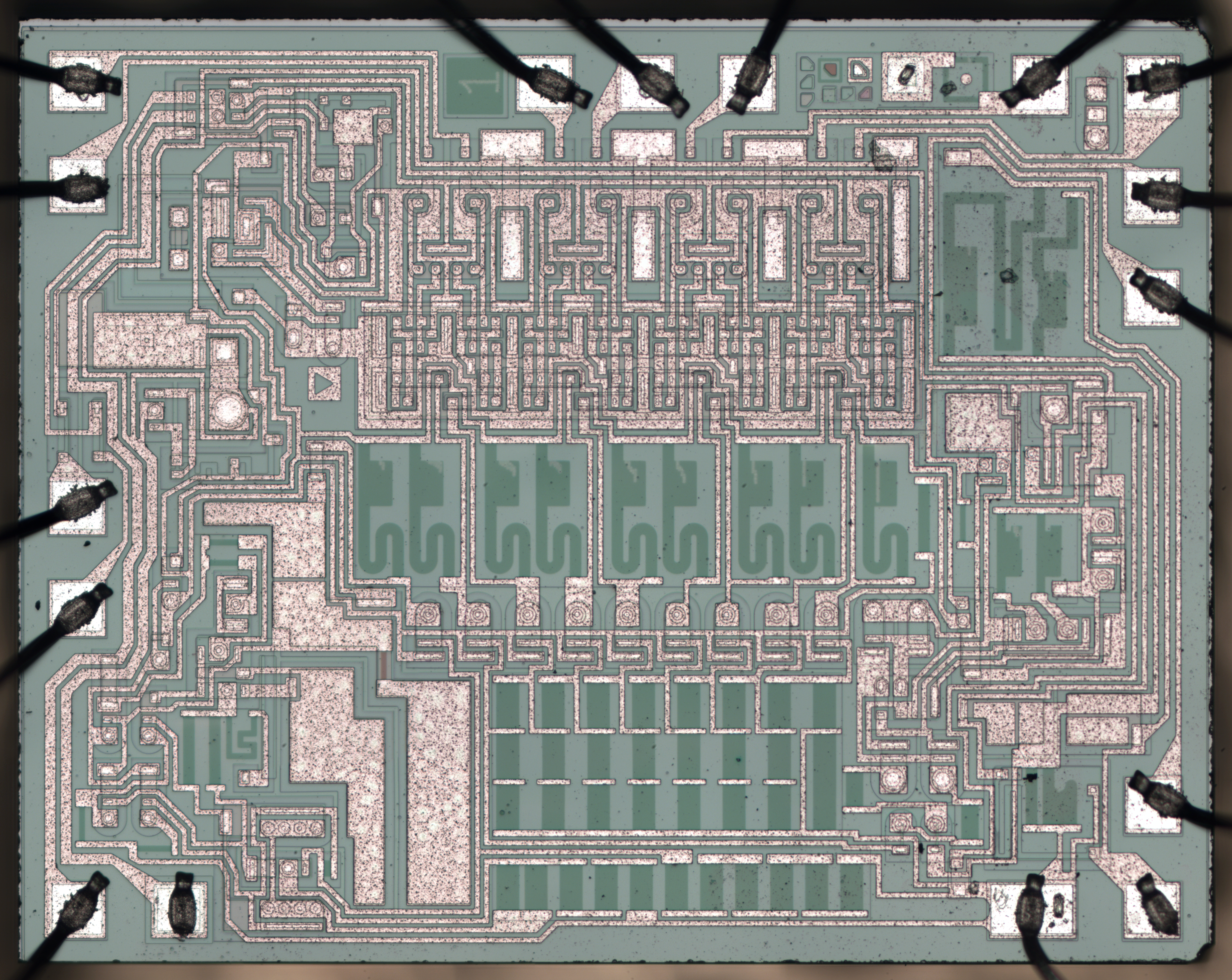
Oh, these rounded resistors are just beautiful... Autorouters in 2014, do you see this?
Note how amount of laser trimming on R-ladder is different for different bits.
PS. Could anyone share position of western engineers on plastic-vs-ceramic package for military/space-grade IC's? It appears modern plastic packages offer more benefits (like better G-shock/vibration reliability and obviously cost) without sacrificing anything (temperature range and moisture are less of a concern now, radiation was never a concern for a package).