May 22, 2014
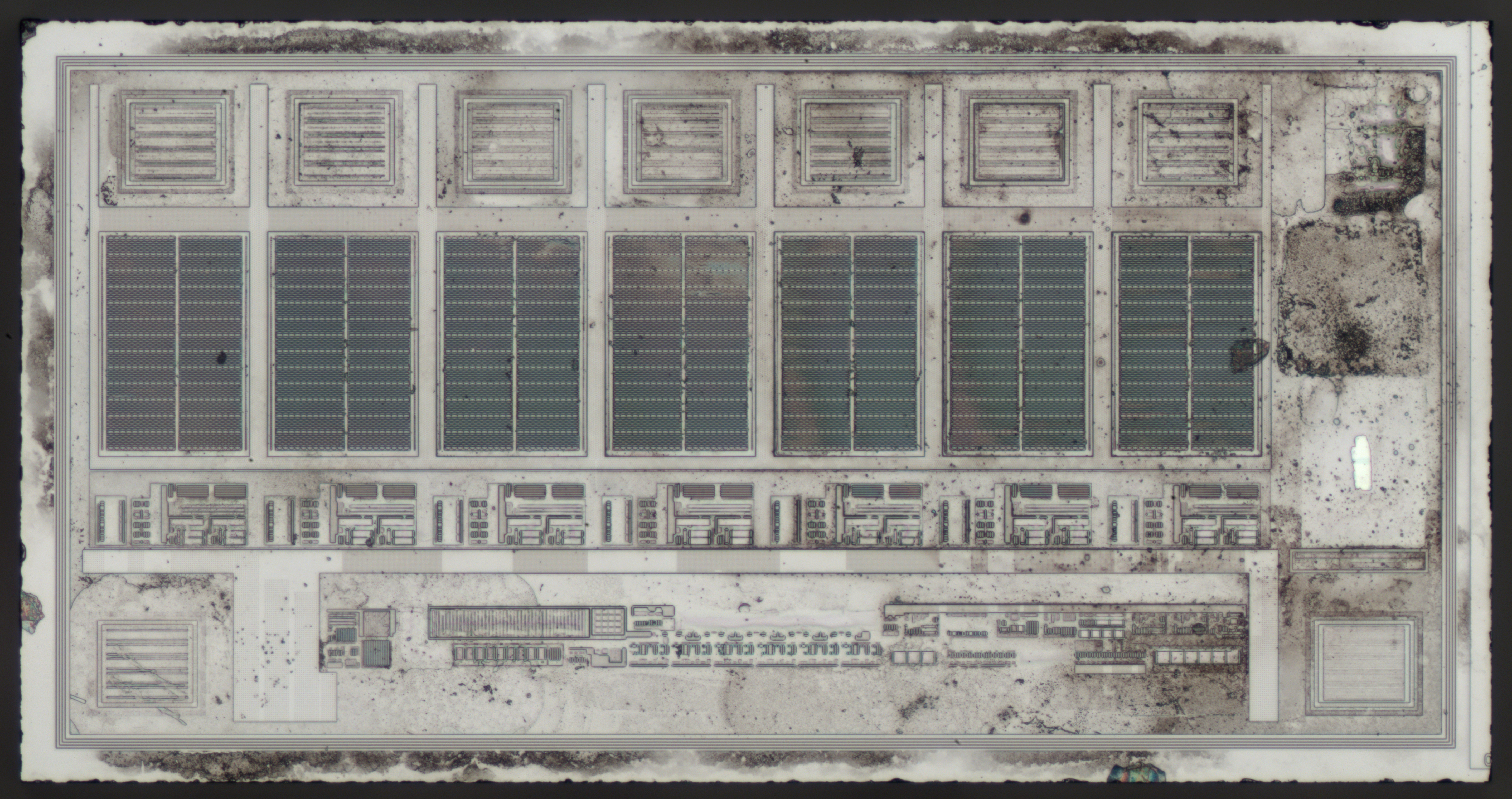
KR580VM80A - getting ready for reverse engineering : weekend die-shot
We decided to take a closer look at the most popular soviet processor KR580VM80A (first shoot), so that group of enthusiasts (russian only) would be able to recover schematic from it's layout.
Read more →


May 17, 2014
Toshiba TCD1201D - linear CCD : weekend die-shot
Toshiba TCD1201D is a monochrome 2048-pixel linear CCD. You can also notice few extra pixels for calibration shielded with aluminum.Die size 34814x802 µm.

With this die we've reached JPEG limits, full image would be 80k+ pixels wide, so we'll show beginning and the end of the CCD separately:
We are grateful to Kony for this chip.
May 3, 2014
SkyWorks AAT4292 - 7-bit high-side IO expander: weekend die-shot
SkyWorks AAT4292 is a 7-bit IO expander with 100mA 1.1Ω high-side switches per channel.Die size 1193x618 µm.
After metallization etch:
April 12, 2014
Phillips PCF8574 - 8-bit I2C port expander : weekend die-shot
Phillips PCF8574 is 8-bit I2C port expander, 3µm manufacturing technology.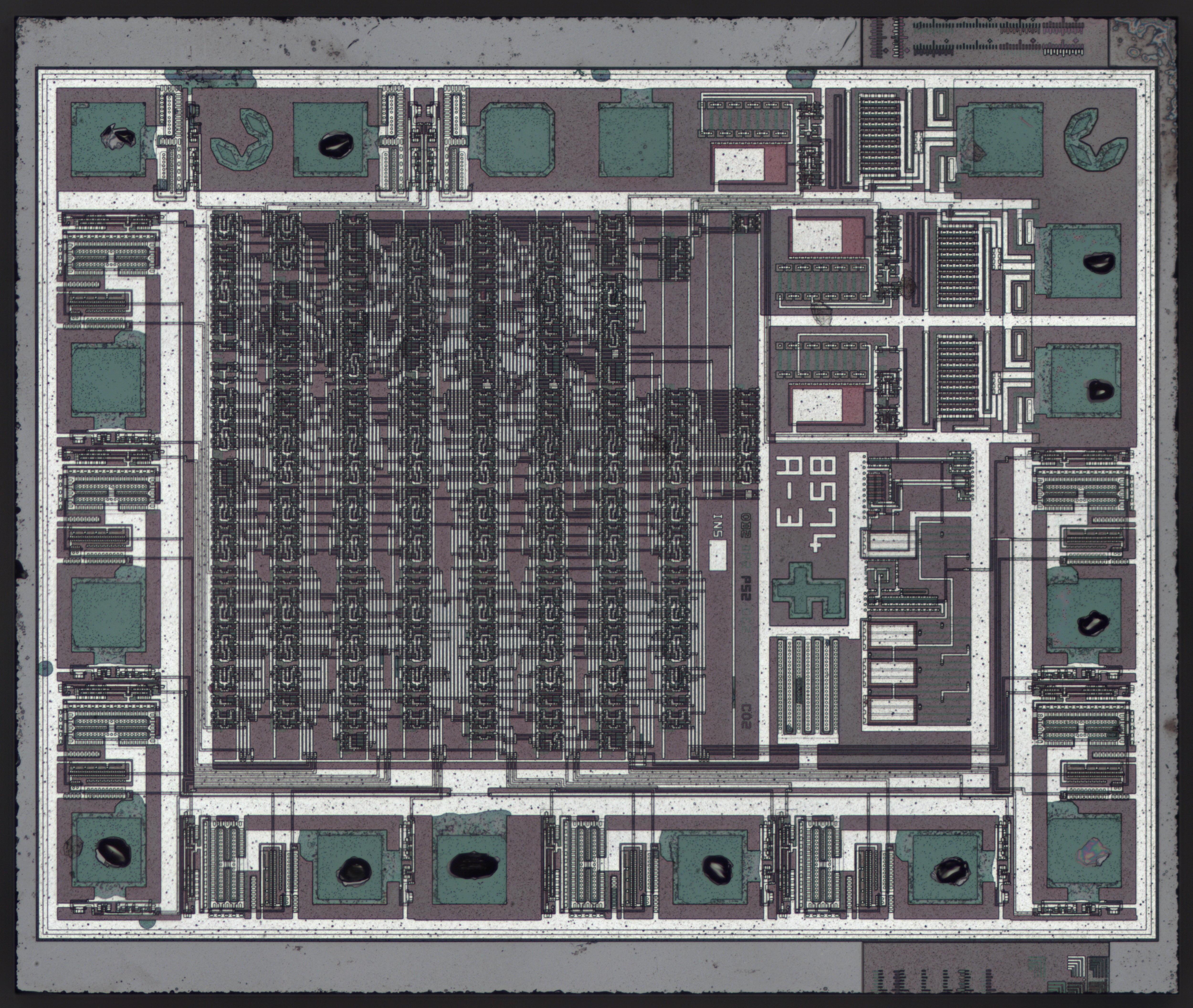
April 8, 2014
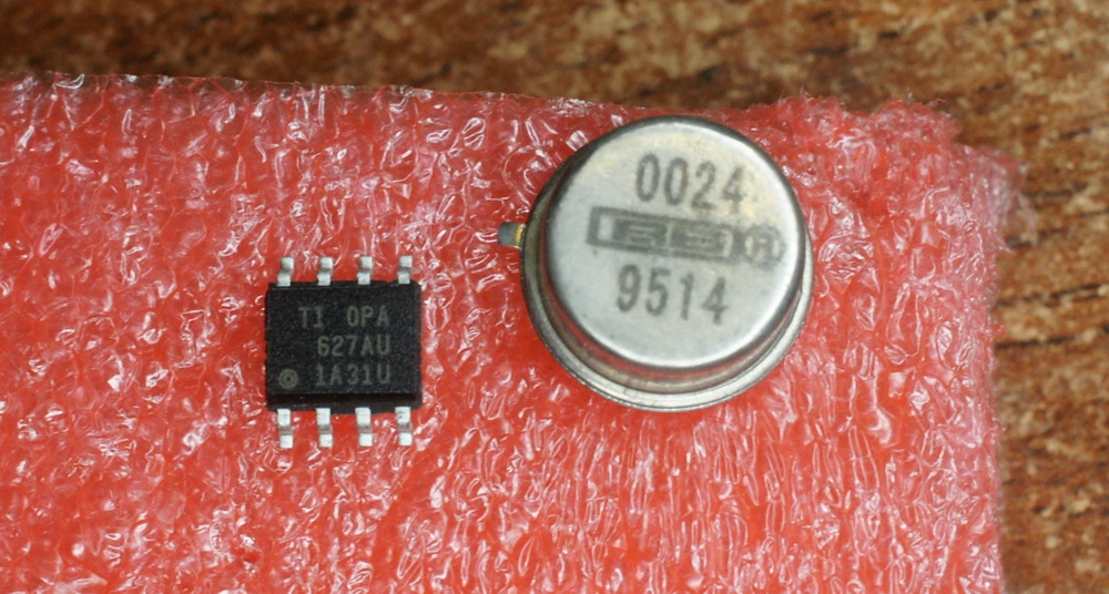
Fake audiophile opamps: OPA627 (AD744?!)
Obviously, something fishy was going on. I ordered one, and for comparison - older one in metal can package, apparently desoldered from some equipment. Let's see if there is any difference.
Read more →
March 29, 2014
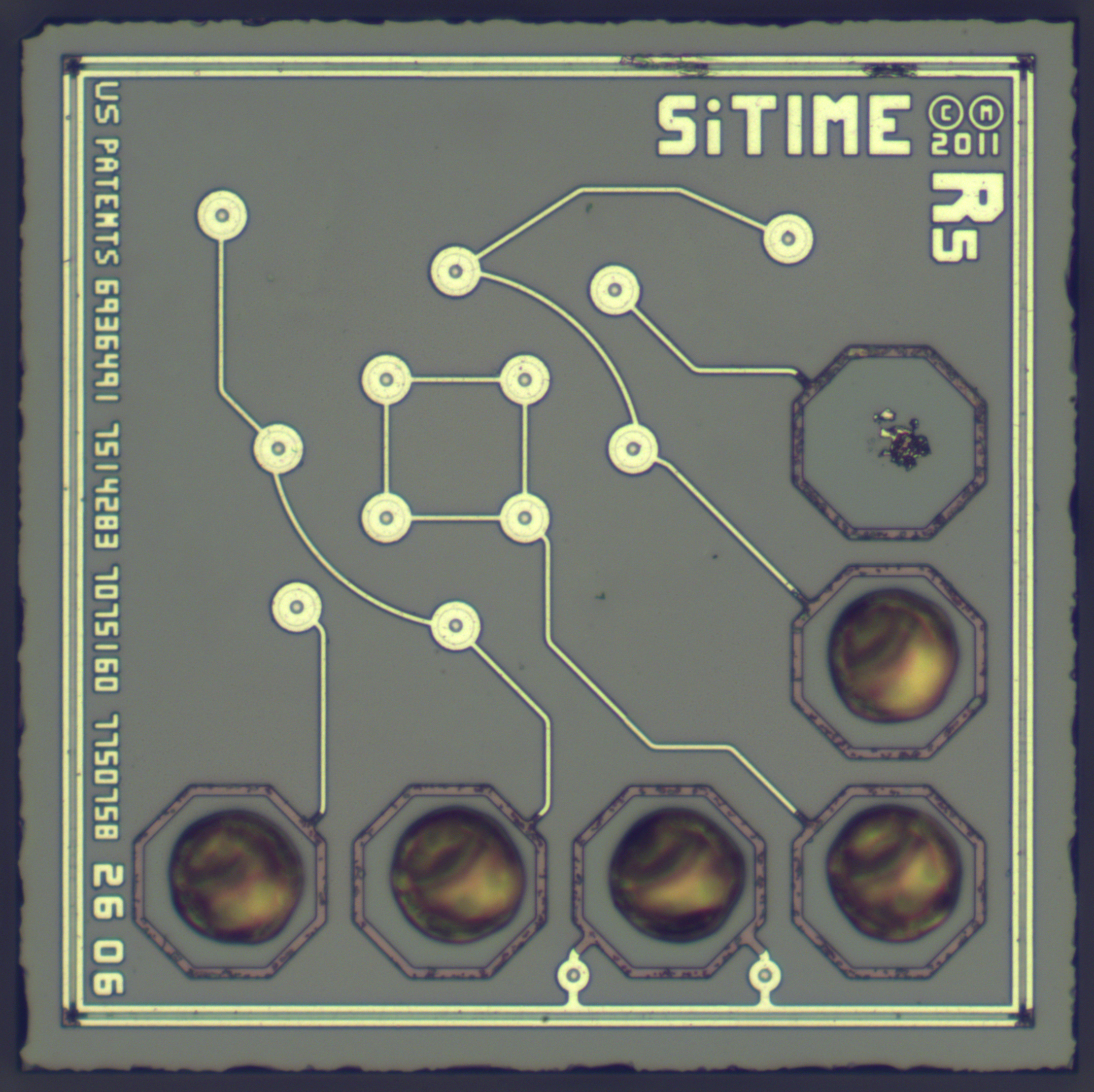
SiTime SiT8008 - MEMS oscillator : weekend die-shot
Photo of MEMS die puzzled us for quite some time. Is it some sort of integrated SAW/STW resonator?
The trick is that to reach maximum Q-factor (up to ~186'000 according to patents) MEMS resonator must operate in vacuum. So they package resonator _inside_ the die in hydrogen atmosphere, then anneal it in vacuum so that hydrogen escapes through silicon. So we see here only a cap with contacts to "buried" MEMS resonator. We were unable to reach the resonator itself without x-ray camera or ion mill.
MEMS die size - 457x454 µm.
Thankfully relevant patents were specified right on the die : US6936491 US7514283 US7075160 US7750758 :)
Read more →
March 22, 2014
TI TL431 adjustable shunt regulator : weekend die-shot
TI TL431 is an adjustable shunt regulator often used in linear supplies with external power transistor.Die size 1011x1013 µm.