
May 2, 2013
1986VE91T: What's inside Russian ARM?
1986VE91T (1986ВЕ91Т in Russian) - is an ARM Cortex-M3 based microcontroller, designed by Russian company Milandr. It has 128 KiB of flash memory, 32 KiB of SRAM, hardware USB and 80Mhz core clock. Manufactured using 180nm technology with aluminum metalization.As this chip was in ceramic package, no plastic etching was necessary - so all bonding wires are intact. Die size - 6.54x5.9 mm.
Etching metalization, almost there...
Now we've reached polysilicon level:
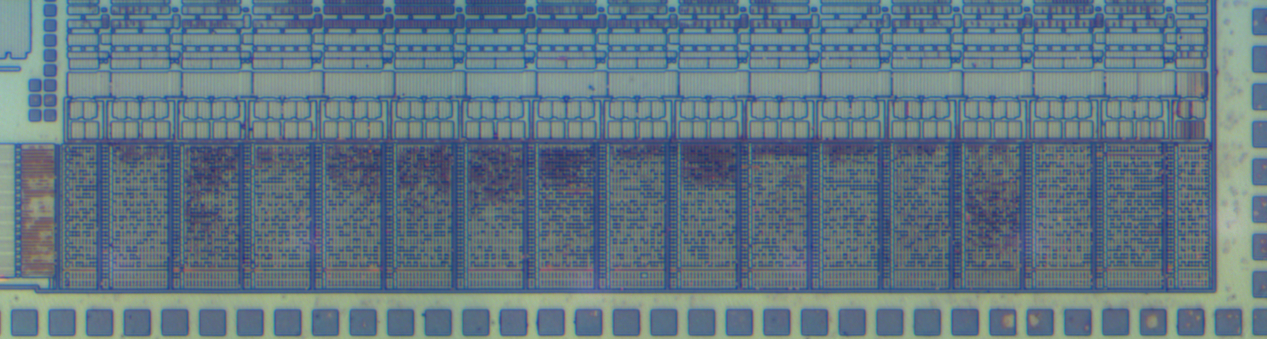
Die annotation
IO Cells & bonding pads - standard circuits to drive IO pins. Includes ESD protection, can work as in and out pin. There are no transistors below bonding pads - that's because bonding process could damage transistors there.
4x32KiB flash - 4 standard block of flash-memory. Why not 1 larger one? Flash IP compiler was unable to generate memory wider than 32 bit, but 128-bit was required to meet performance requirements.
32KiB SRAM - fast SRAM memory, looses it's content without power.
256x32B ROM - boot memory, programmed via poly-silicone "jumpers". It's so called "mask rom".
USB PHY - physical interface for USB IO. It only has transmitter/receiver, all logic is inside "synthesized logic" part of the crystal.
Internal linear regulator (1.8V) - required to lower power consumption, as 1.8V transistors uses much less power compared to 3.3V ones.
Battery domain - powered from external battery. Designed for minimal possible power consumption. Contains real time clock, oscillator for external 32 kHz crystal, and few bytes of memory.
RC Oscillators - internal generators (low speed and high-speed), allows to use microcontroller without crystal.
System/USB PLL - allows to multiply RC/crystal clock to get required frequencies for system and USB controller.
2xDAC - digital->analog converters.
2xADC - analog->digital converters. Apparently empty places were capacitors.
FIFO/Buffers - small blocks of static memory. Most likely these are FIFO buffers for dual CAN controllers and others.
One does not need to design most of the blocks above - it is a common practice to license already designed & tested pieces.
Cell based synthesized logic - automatically synthesized digital circuit from Verilog description. Both microcontroller core and digital part of peripherals are there. Also, instead of drawing transistors directly, synthesis software just places standard cells, and then automatically routes connections between them. Standard cells has the same height, but different width, and implement simple logic functions like AND, OR, trigger, e.t.c
Closer look
Boot ROMOne could extract boot rom content here. In this case it's not really necessary, as it's accessible in debug mode.
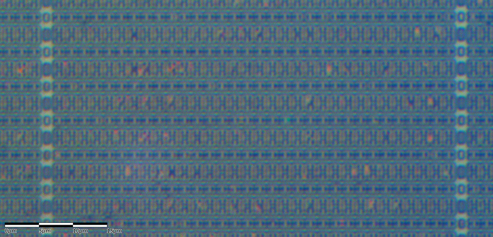
SRAM
Cell size 9.14 µm2, matches 180-250nm technology.
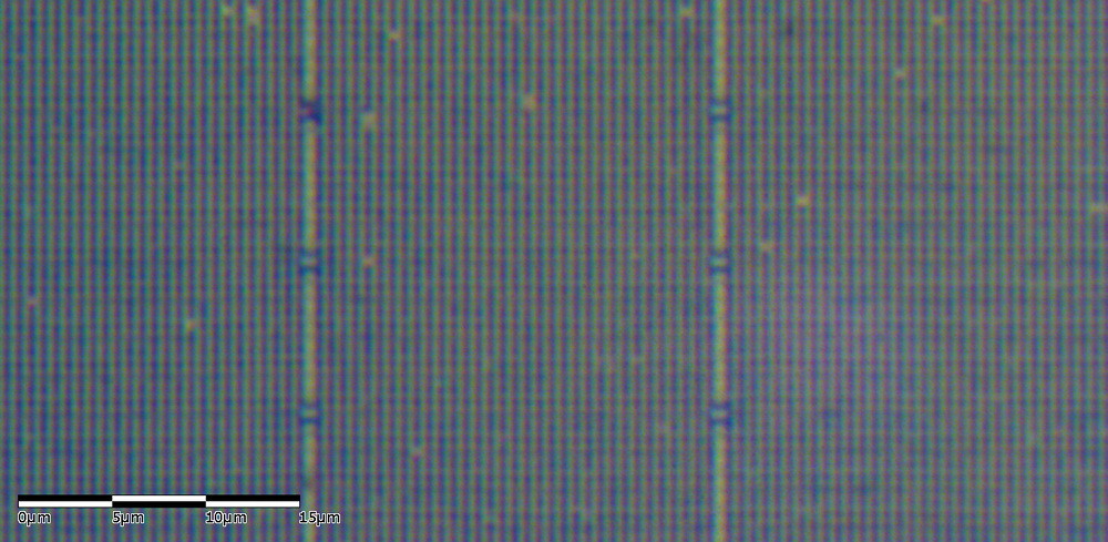
Flash
You can see that cell size is much smaller - as it only needs 1 transistor per bit (compared to 6 for SRAM):
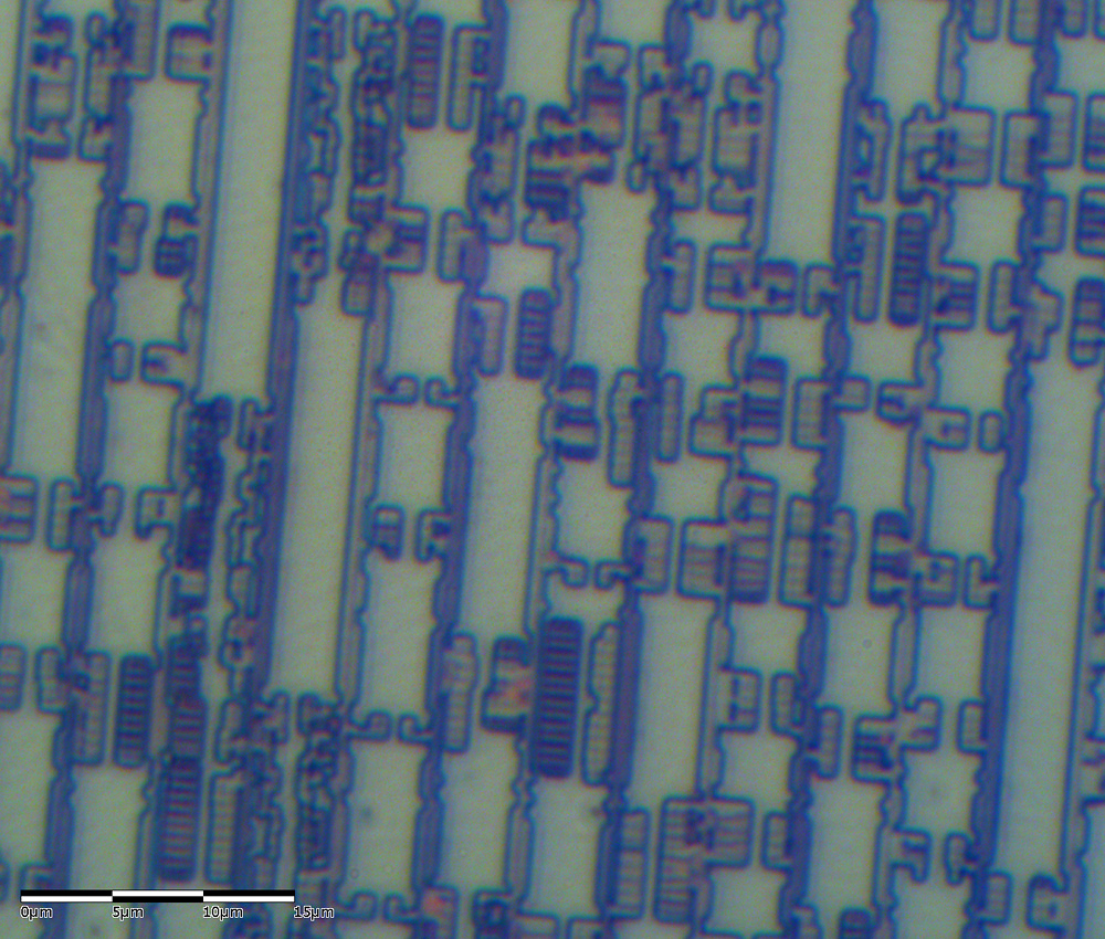
Synthesized logic
And here we see columns of standard cells, implementing microcontroller core and peripherals. Of course, now it's impossible to guess function of each cell as all metal interconnect was etched away.
Hopefully that was interesting - follow us on Twitter @Zeptobars or subscribe to our RSS feed - we'll continue opening chips.


