
August 11, 2013
ULN2003 - practical example of «reading» microchip schematic
Despite it's simplicity this microchip is still widely used and mass manufactured. ULN2003 contains 21 resistors, 14 BJT transistors and 7 diodes. It is used to control relatively high load (up to 50V/0.5A) from microcontroller pin. Canonical use case - controlling segments of large 7-segment LED displays.
ULN2003 die photo
Colors are more saturated, metal under contact pads is damaged by acid and became brown.Die size is 2.53x1.71 mm.

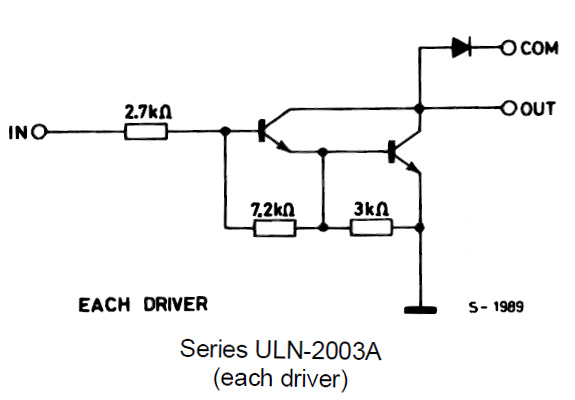
As we can see all 7 channels are identical, so we'll be analyzing only 1. Fortunately for us schematic is also available, so we can use it for reference:
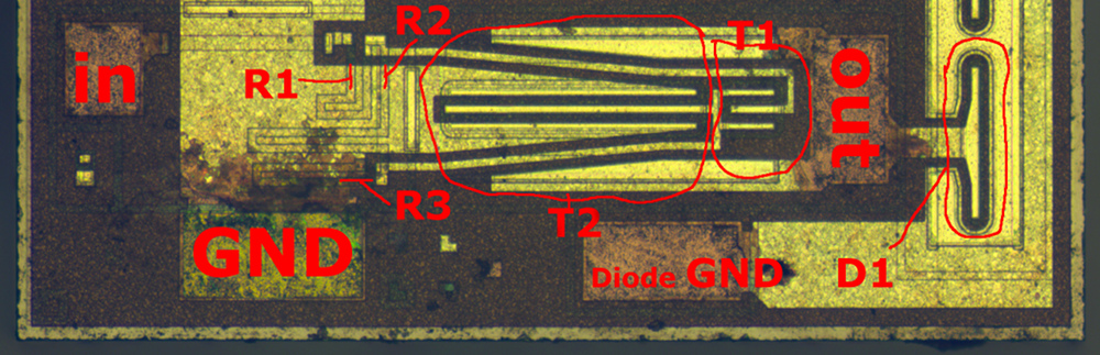
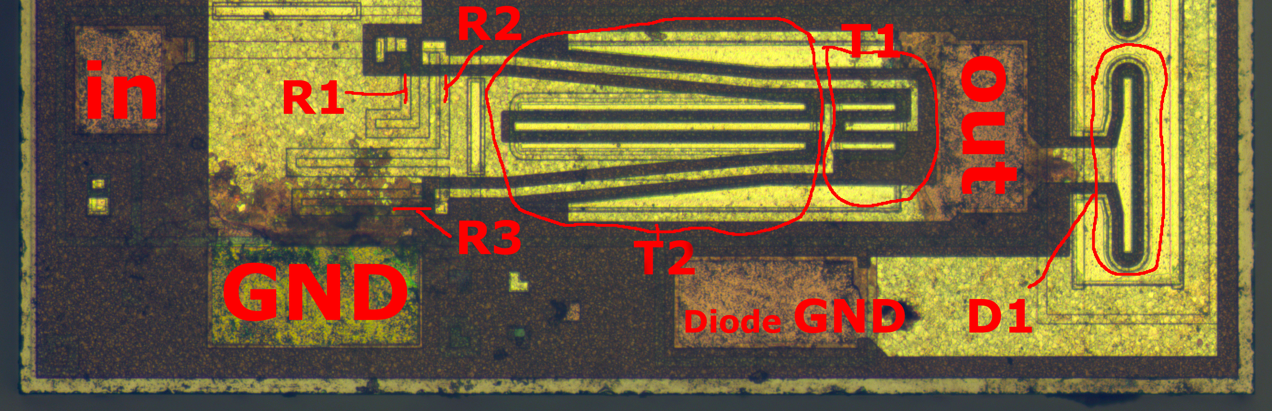
And now closeup of 1 channel with all elements annotated. I'll leave it as an homework task to figure out mapping between schematic and layout.
Note that while common diode connection is called "Diode GND" it's usually connected to supply voltage - so these diodes make sure that output voltage would not be higher than supply voltage (this might be important for inductive load).
But how individual transistor is made? it is known that cross-section of planar BJT npn-transistor looks like this:

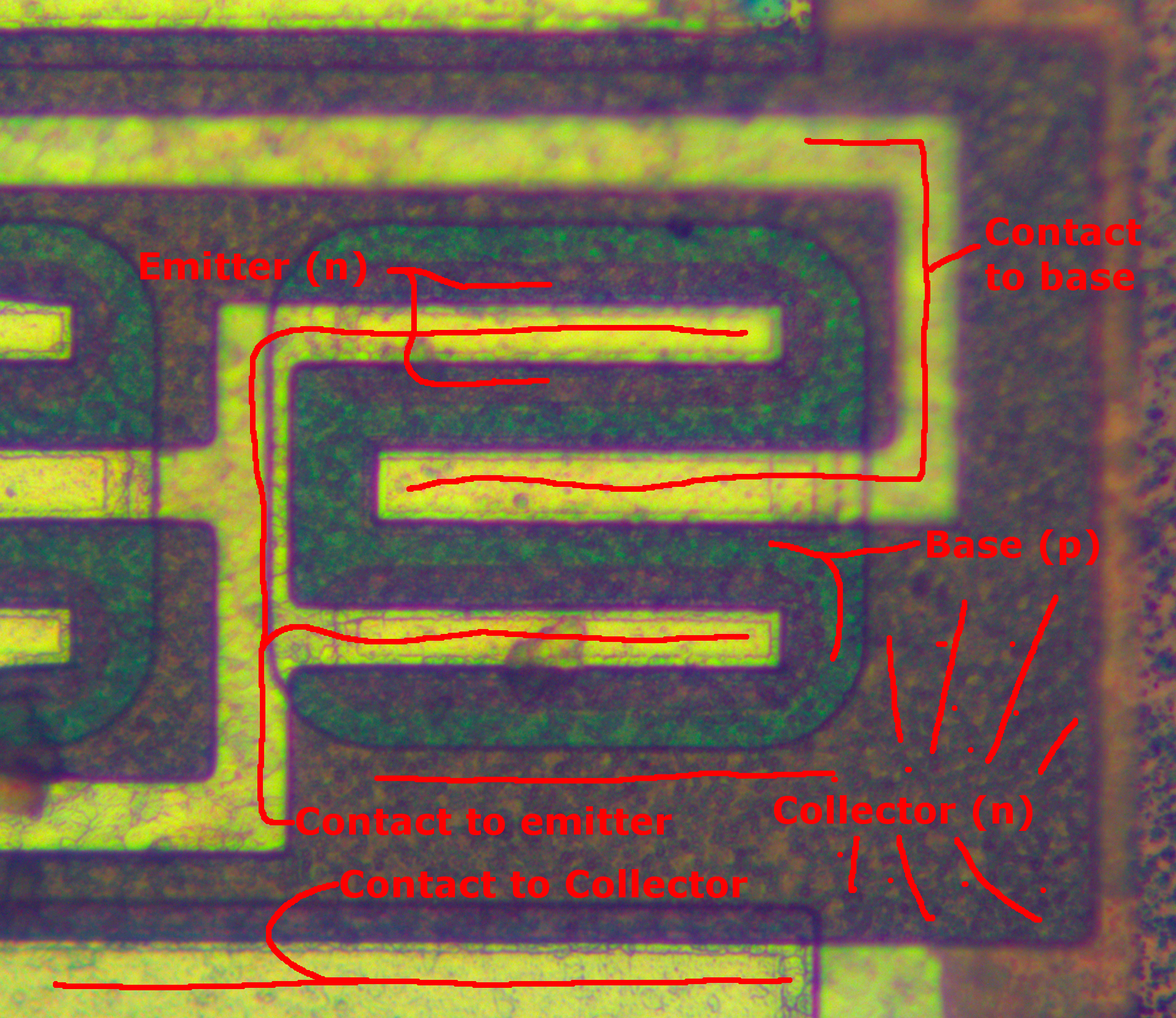
Thin base goes under emitter. While emitter and collector are both n-type silicon, they are not equivalent. Doping concentration and thickness are optimized for "current amplification" in 1 direction only.
Now we can take a look at individual transistor and try to figure out how it is designed. P and N-type silicon has slightly different color. This difference is quite small, but after cranking up saturation and contrast almost to the maximum we can clearly distinguish between them. Don't worry about dual emitters - they work just like 1 with combined area.
In order to avoid aluminum interconnect shorting wrong parts of the transistor - it is covered by a layer of insulating transparent glass. This glass has holes right above places where interconnect is supposed to contact the transistor. You can clearly see this on the following photo made with a lens that has narrower depth of focus: base contact is out of focus as it's laying higher, on the transparent glass.
Collectors of both transistors in same channel - is effectively same piece of silicon. This is ok because on the schematic collectors are connected. Different channels are insulated by pn-junction between them - it works like a pair of diodes not allowing current to flow to neighbor channel. You can see these insulating "doped rectangles" on higher-resolution photo
Now you can see that there is no magic smoke inside :-)


