
July 11, 2015
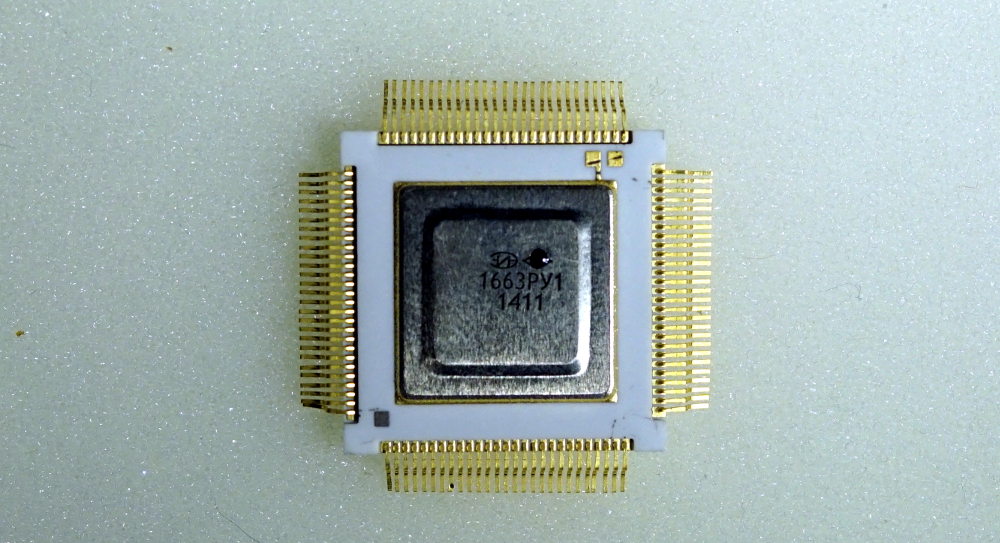
Mikron 1663RU1 - first Russian 90nm chip : weekend die-shot
Mikron is currently the most advanced microelectronic fab in Russia, located in Zelenograd. In 2010 they have licensed 90nm technology from STMicroelectronics, and equipment setup was somewhat ready by the end of 2012. Technology transfer was hindered by very small manufacturing volume and scarce funding. Nevertheless, 1663RU1 has became their first 90nm product reached commercial customers. It's 16 Mibit SRAM chip.There are no redundancy or ECC correction on this chip, bulk-Si technology ("civilian" technology). There are no radiation-hardening tricks implemented. This chip is apparently intended for industrial/military applications, use in space is only possible with great care.
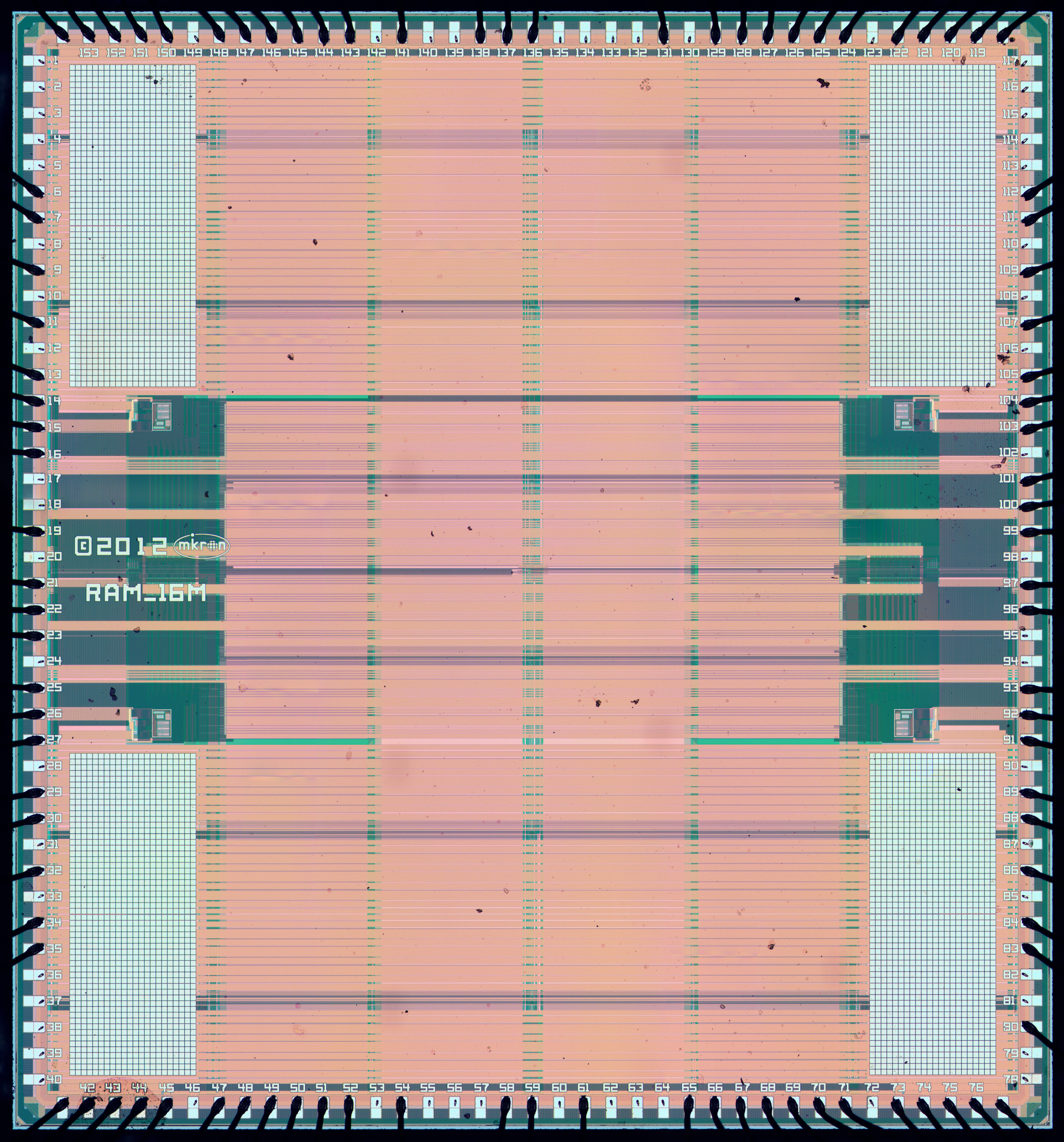
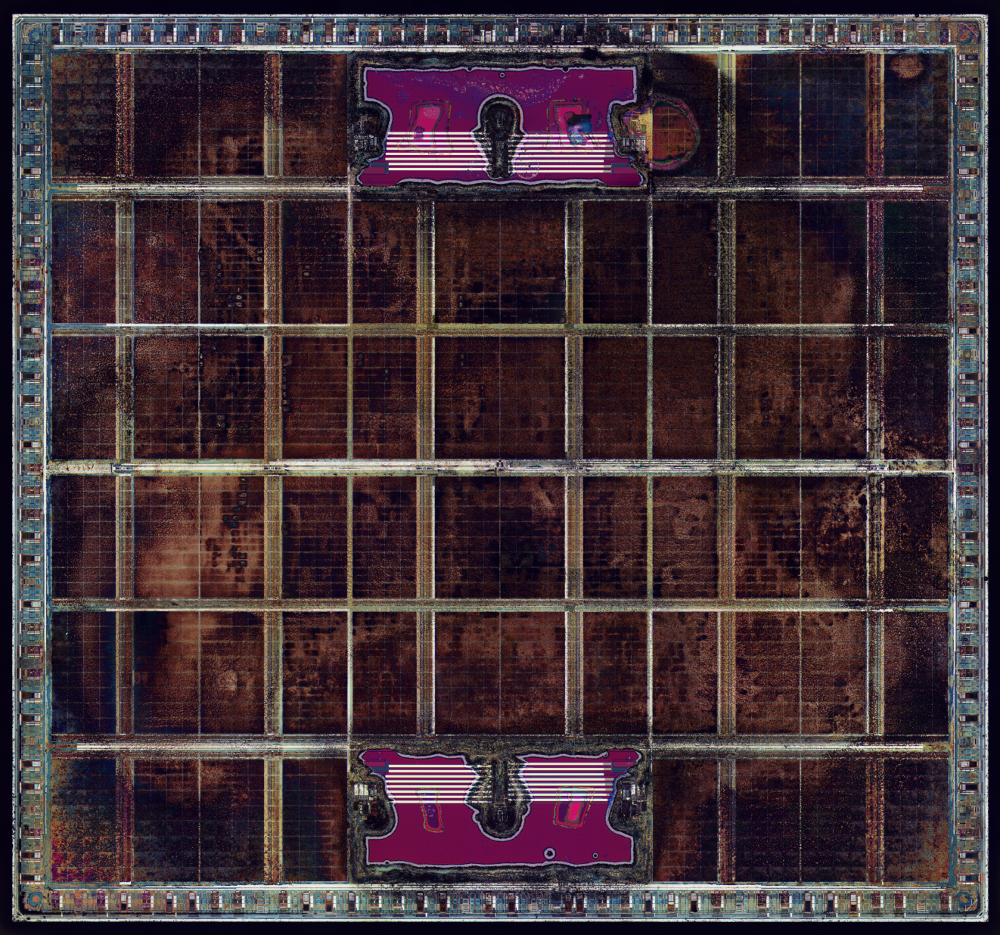
After metalization etch. Each small square is a matrix of 64x128 bit, 16 Mibit total.
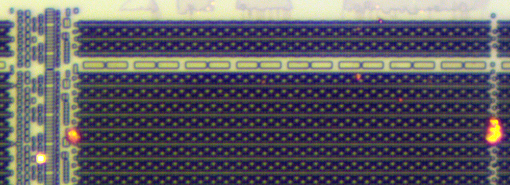
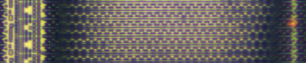
Finally, SRAM cells itself. Cell area is 1.2 µm2, which is average level for 90nm tech (best ones are 1um2). Scale is 1px=57nm.
For comparison 180nm SRAM from ST Microelectronics in the same scale (STM32F100C4T6B).

If we take a look at the piece where bits of first metal preserved, we can see that Mikron is using litho-friendly SRAM design, where critical levels only use straight lines.
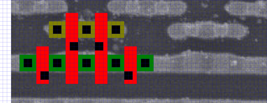
Here is Andrew Zonenberg's suggestion on 6T SRAM cell layout:
Die size 5973x6418 µm.


