December 29, 2013
Invensense MPU6050 6-axis MEMS IMU : weekend die-shot
MEMS is probably the most requested thing we are asked about. Year ago we unsucesfully tried to take a photo of MPU6050. Now it's time for revenge!Invensense MPU6050 is an integrated gyroscope and accelerometer with 16-bit readings. It contains 2 dies, soldered/welded face-to-face in multiple places (that's what was causing us troubles last time, required temperature for separation exceeded 600C).
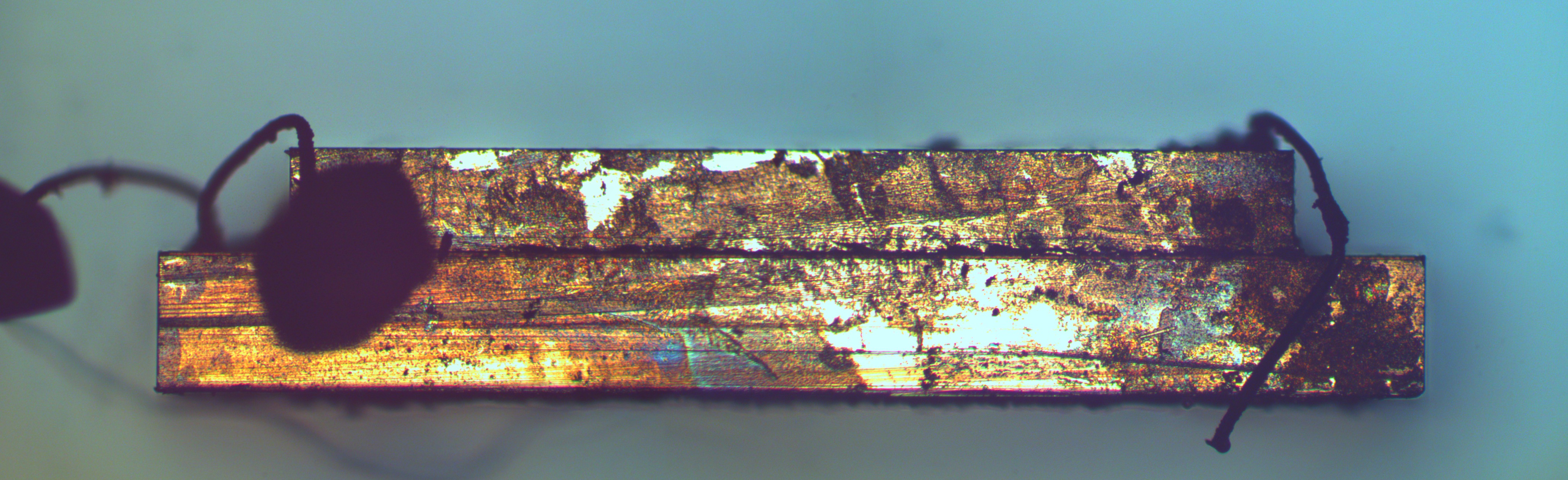
On the overview photo you can see how not-flat they are. On a bigger die MEMS part is 28µm above surface, on smaller die - 100 µm above. Also, there is logic right under MEMS on the bigger die.

Size of big die is 2782x2718 µm, small die - 2778x2195 µm.
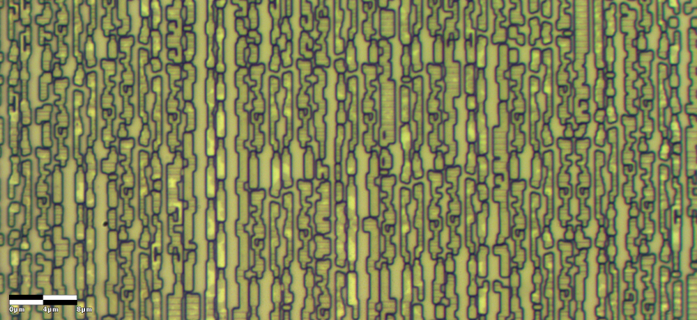
Small die, focus on top level. Width of smallest teethes is 1µm.
These teethes allow to sense their movement by change of capacitance between electrodes.
Small die, focus on bottom level:
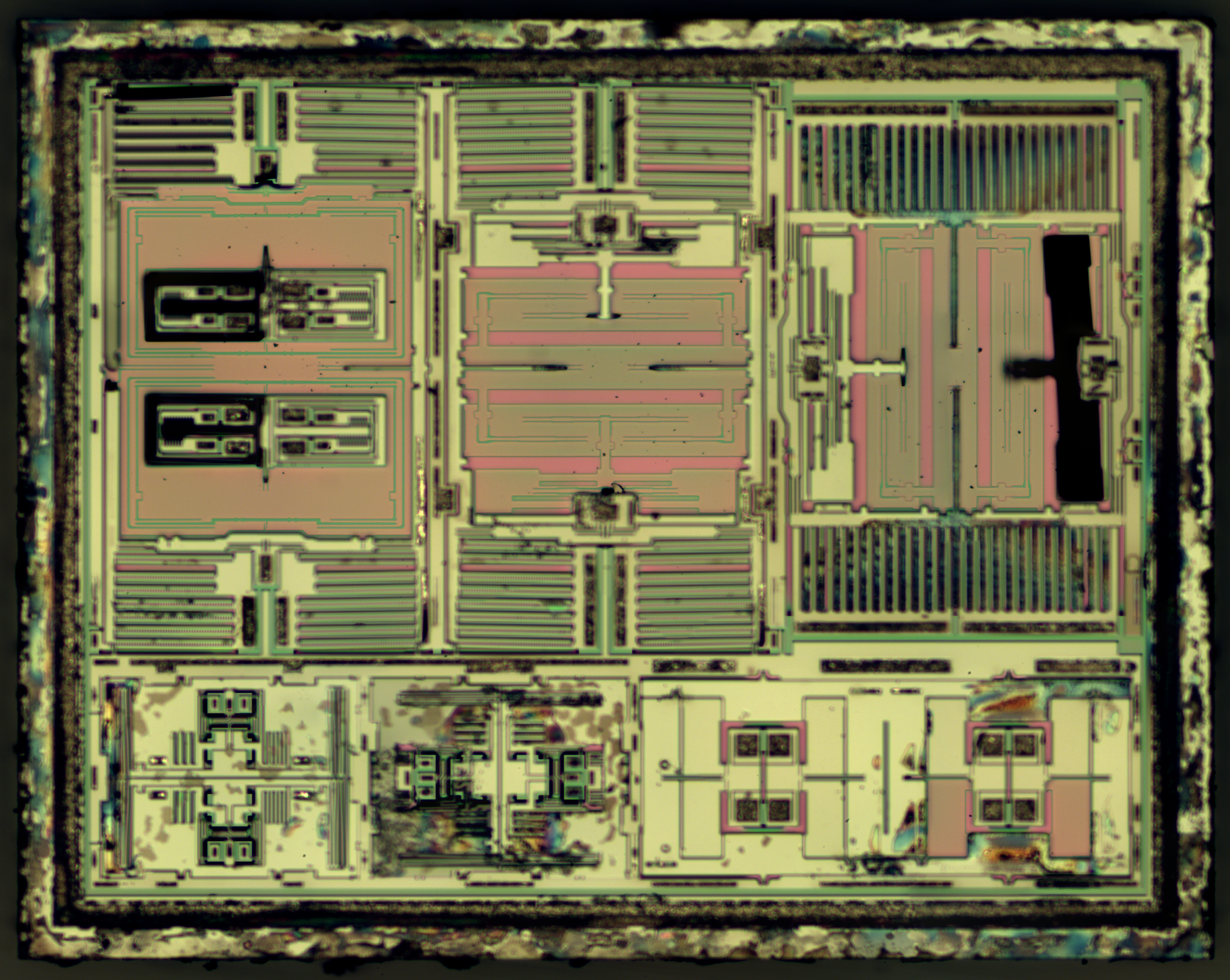
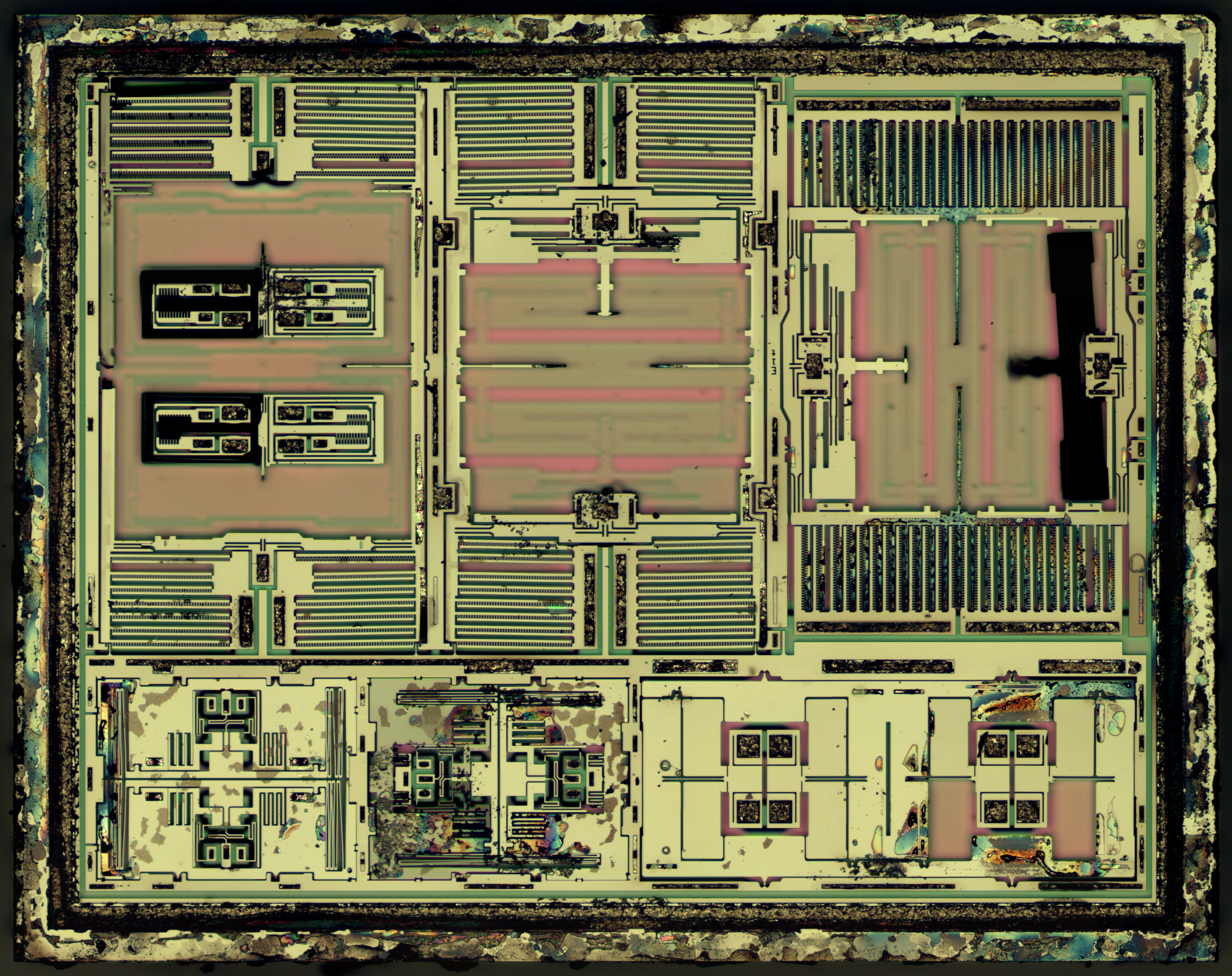
Big die:

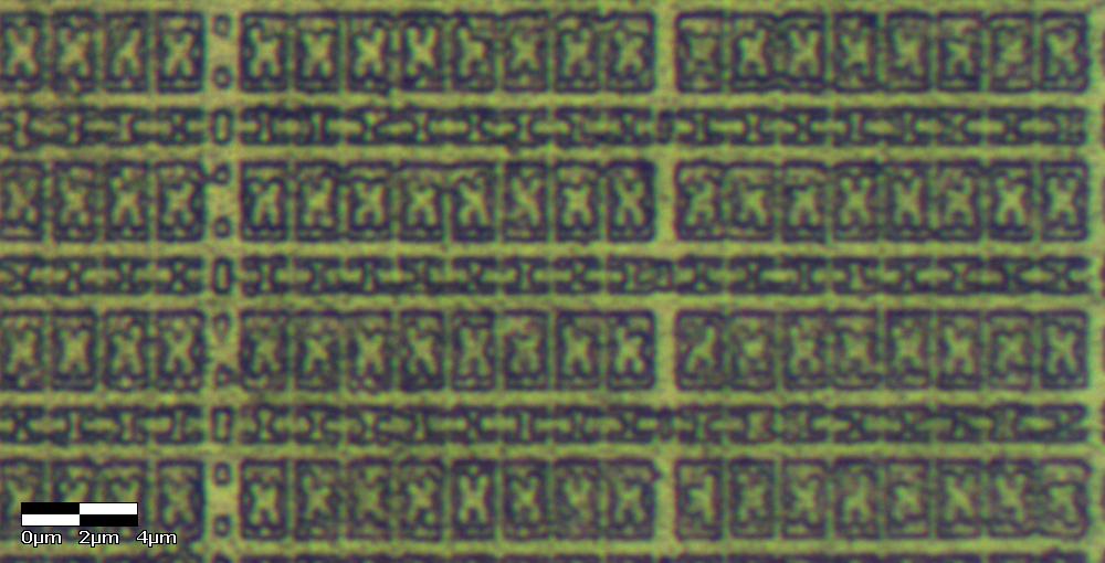
Below MEMS one can find conventional digital logic, ~250nm halfpitch
SRAM, cell area is 10.13 µm2:
Standard-cell-based logic: