February 21, 2013
MSP430F122 : Weekend die-shot
MSP430F122 - 16-bit microcontroller made by Texas Instruments. What's interesting is that die is marked as MSP430F123, with larger flash size.


February 21, 2013
K565RU5 : Weekend die-shot
K565RU5 (pin-compatible to 4164 DRAM chip) - 64 Kib DRAM chip, heart of most of amateur computers made in late soviet times and early 90's. There was also RU7 chip (256 Kib) but it was hard to buy.Die size 5645x2612 µm.
February 11, 2013
Moscow's metro MIFARE/RFID chip : Weekend die-shot
Since February 2013 you can find Sitronics-Mikron's RFID chips inside Moscow's metro tickets, instead of NXP ones which were used before.Mikron chip is 20% smaller. Die size 610x526 µm.

Significant part of chip area is used by passive components:

January 24, 2013
Multiclet MCp0411100101 : Weekend die-shot
Multiclet - basically is a superscalar processor (4-wide at present) with out-of-order execution. 100 Mhz clock, 180nm tech. node, designed in Russia.Die size - 10.2x10.2 mm.
After metallization etch (warning, high-resolution image might kill your browser):
SRAM cell size - 21.28 µm2. So, each of 16 memory blocks contains 72 Kibit of SRAM. Apparently ECC codes are used (72,64). Total accessible memory - 128 KiB.
Autosynthesized standard cell logic:
Test areas were cut with the crystal (resolution test):
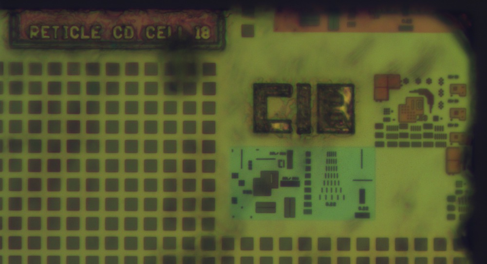
Logo:
January 20, 2013
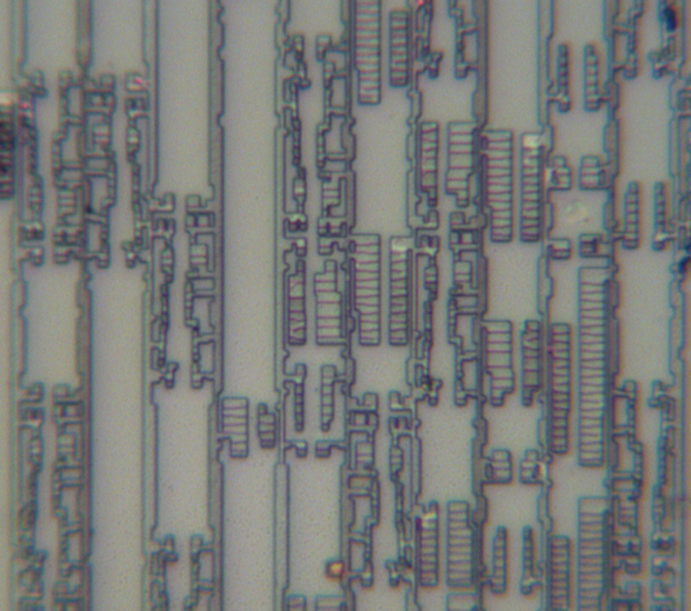
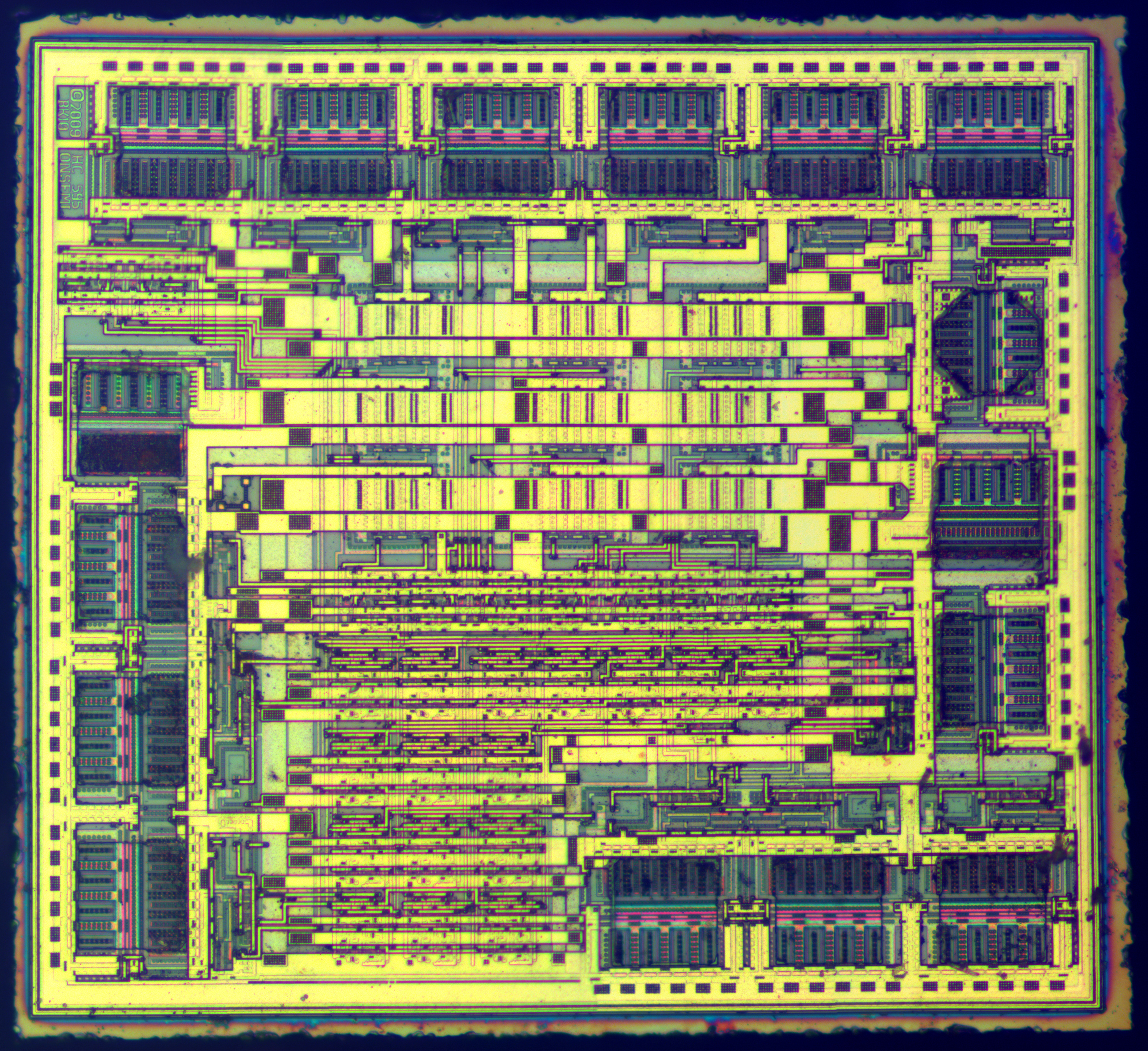
OnSemi 74HC595 : Weekend die-shot
ON Semiconductor 74HC595 is a 8-bit shift register (serial-in parallel-out).That's incredible: 47 years passed since 7400 TTL logic introduction - it is still manufactured and used in new products.
January 20, 2013
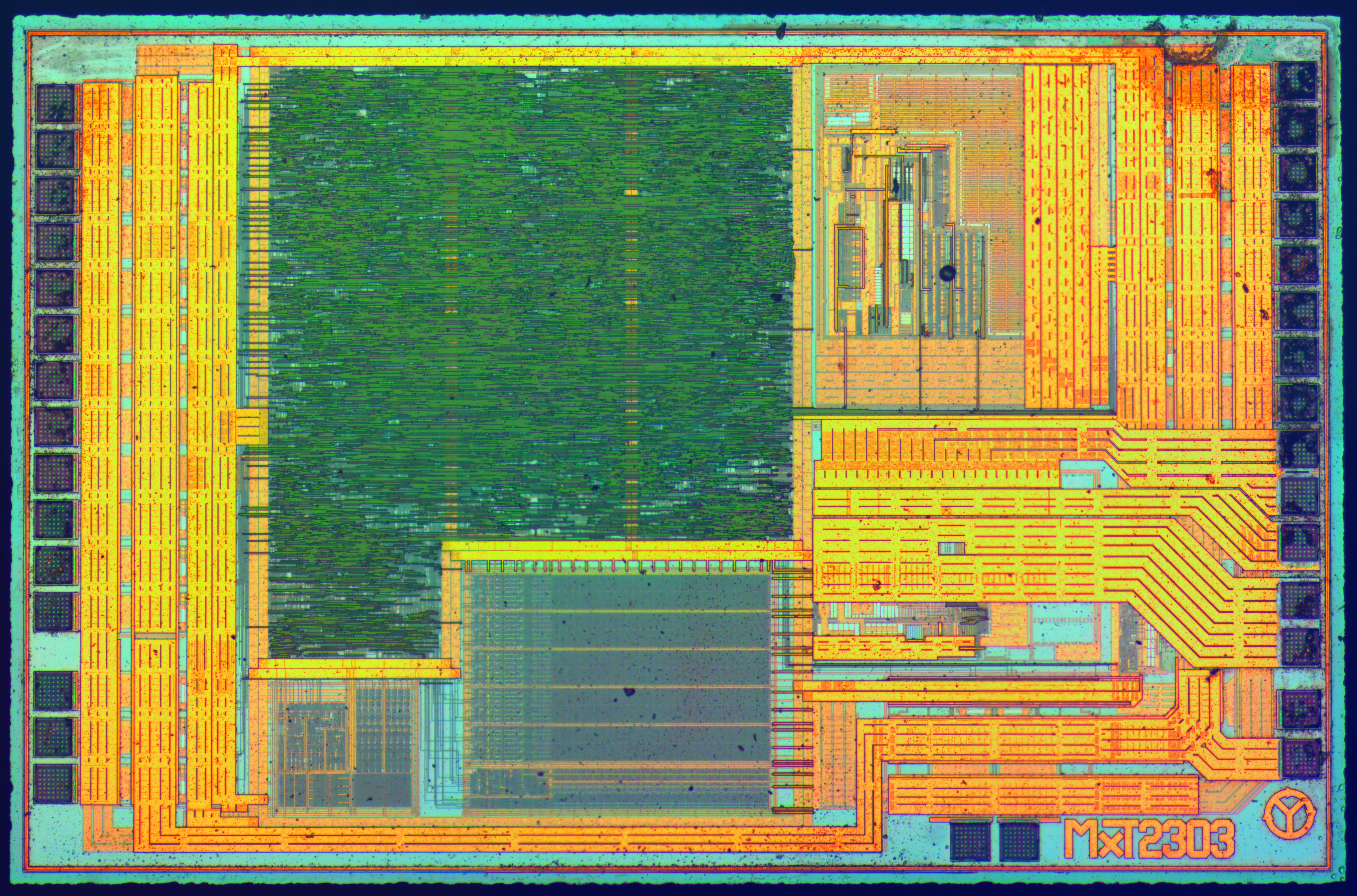
PL-2303HX : Weekend die-shot
PL-2303HX is a USB-to-Serial bridge controller, widely used to connect various electronic devices to PC.Note how wide traces are sectioned so that current does not 'clump up' in the corners.
Die size 5144x3357 µm.
January 10, 2013
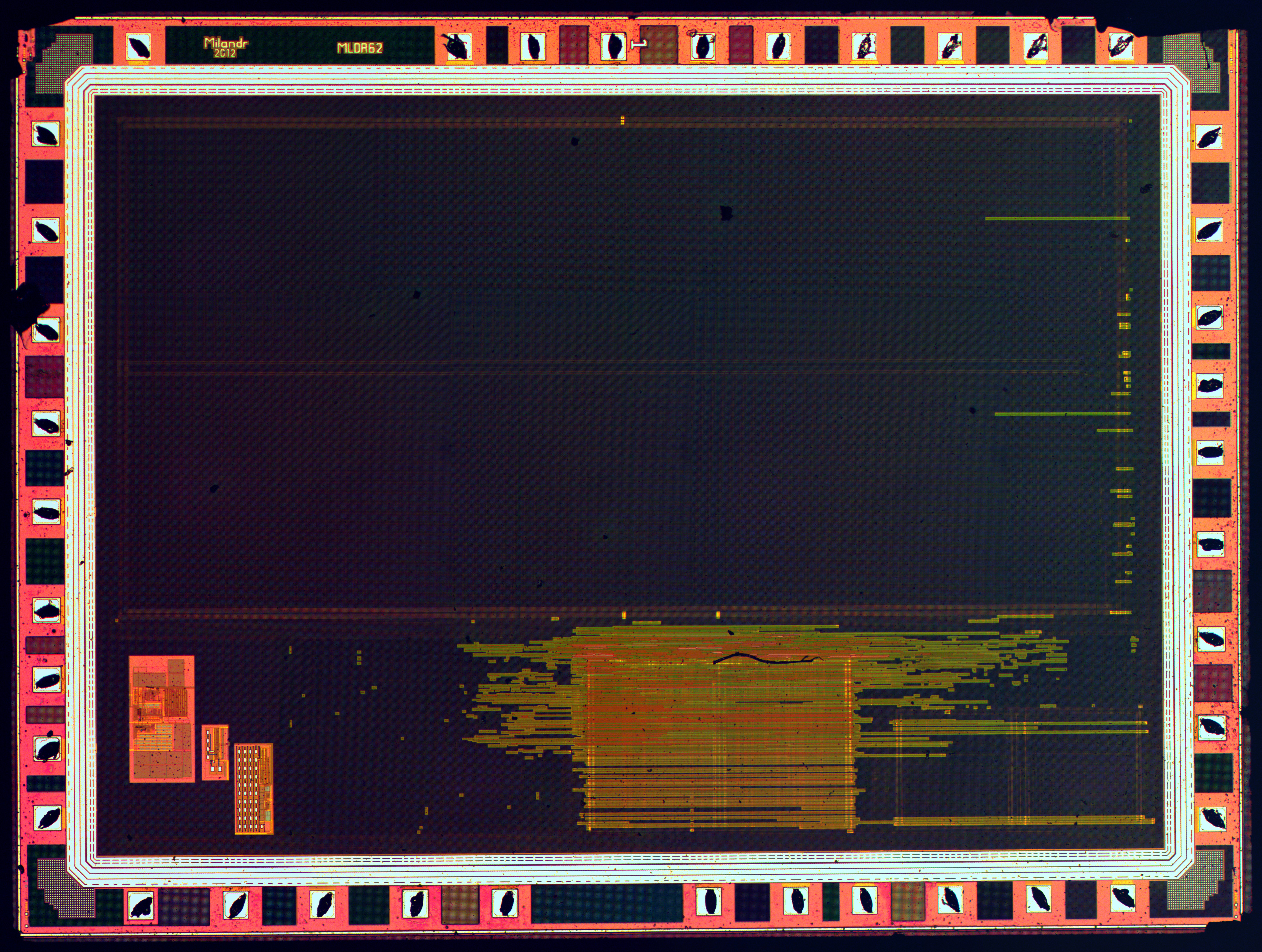
1886VE10 : Weekend die-shot
1886ВЕ10 is a rad-hard 8-bit microcontroller (50Mhz), designed by Milandr and manufactured at Mikron (Zelenograd, Russia).Technology : bulk Si, 180nm with aluminum metalization. Radiation hardening is achieved by using edgeless-transistors and 8T SRAM cells.
Die size 5000x3750 µm.
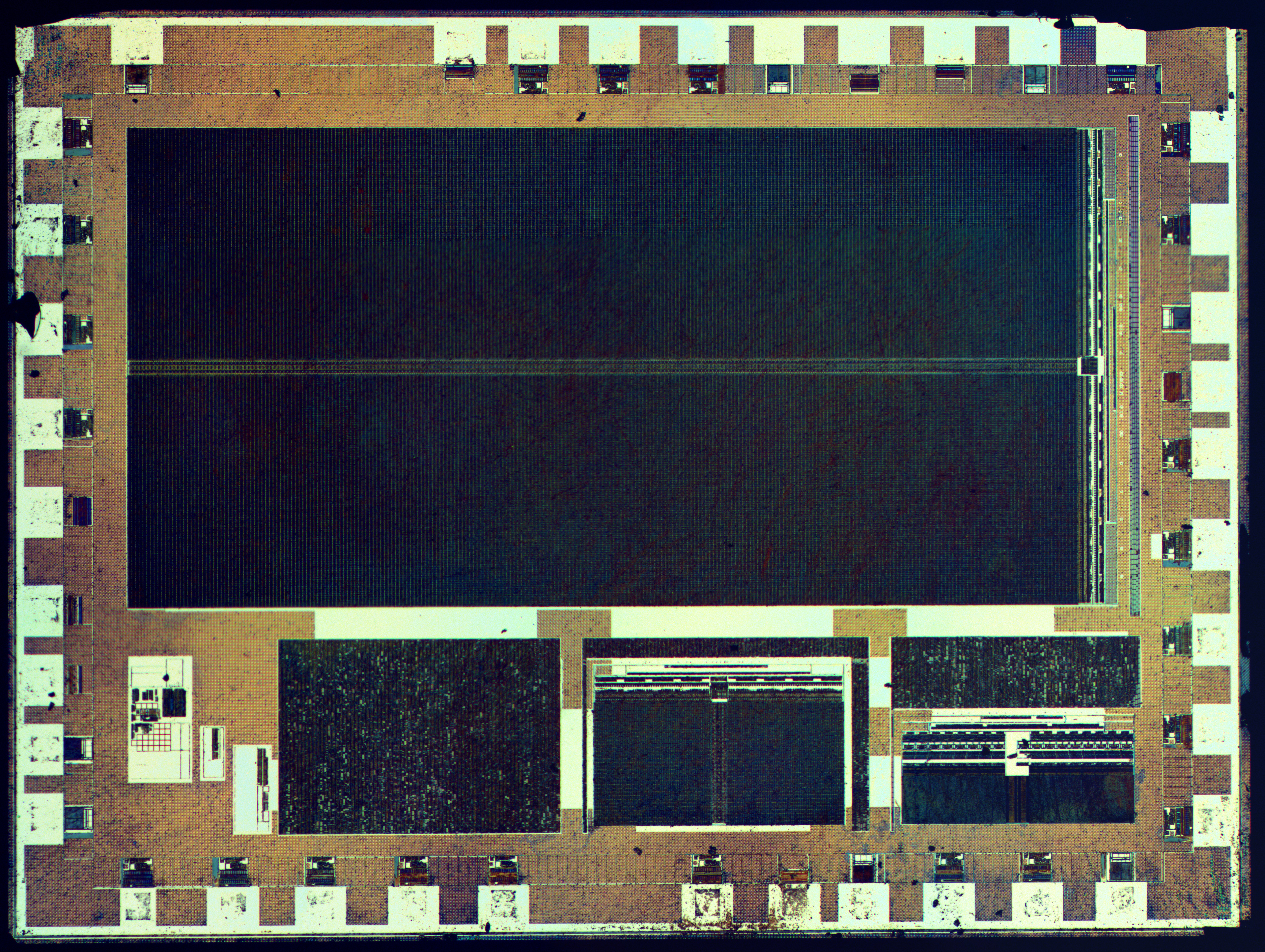
After metalization etch:
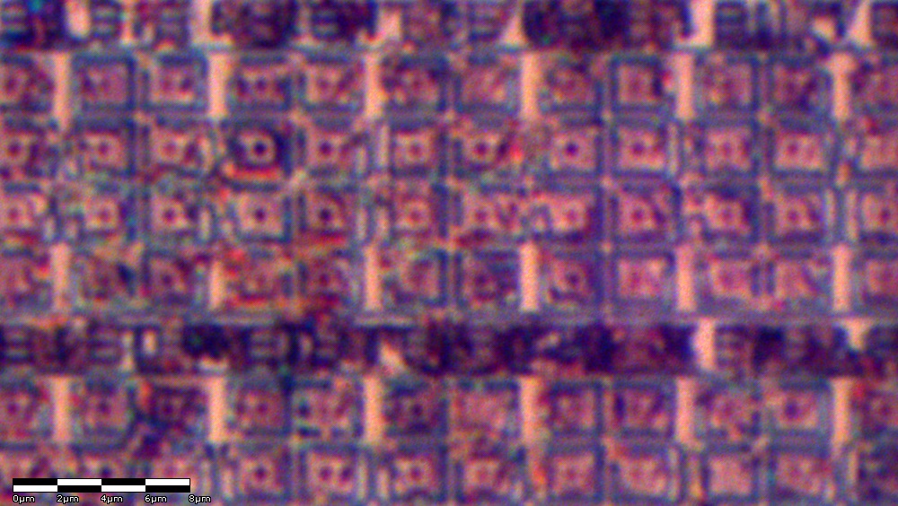
Not much to see using optical microscope:
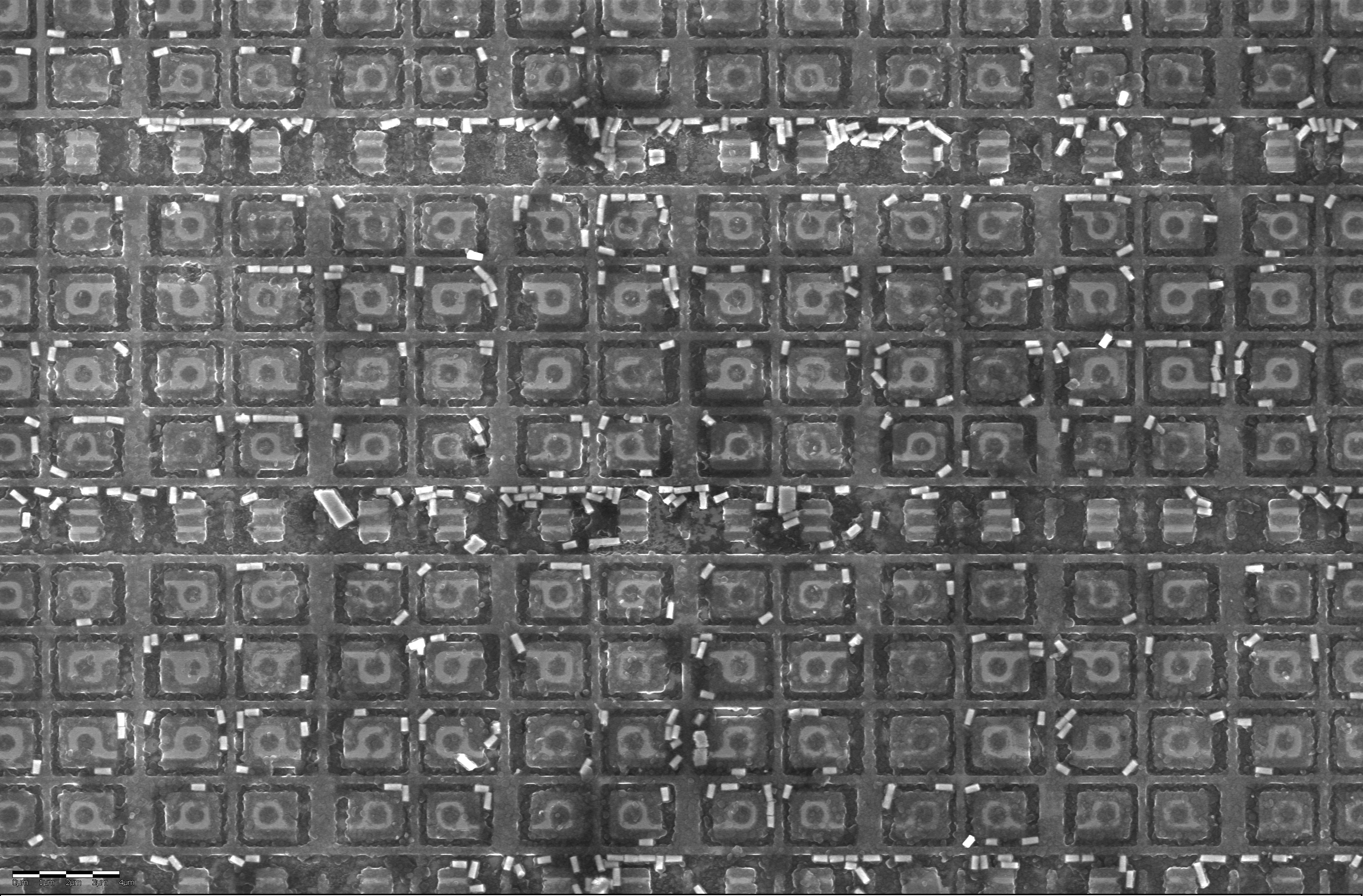
Bright cylinders are tungsten via's left after etching metalization and ILD: