February 17, 2014
FTDI FT232RL: real vs fake
For quite some time when you buy FTDI FT232RL chips from shady suppliers you have a good chance of getting mysteriously buggy chip which only works with drivers 2.08.14 or earlier. We've got a pair of such FTDI FT232RL chips - one genuine and one fake and decided to check if there is an internal difference between them. On the following photo - left one is genuine, right one is fake. One can notice difference in marking - on genuine chip it's laser engraved while on buggy it is printed (although this is not a universal distinguishing factor for other chips).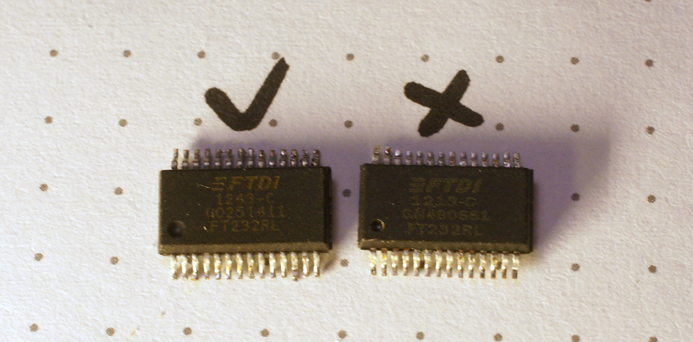
Read more →
January 17, 2014
ST 34C02 - 2048-bit EEPROM : weekend die-shot
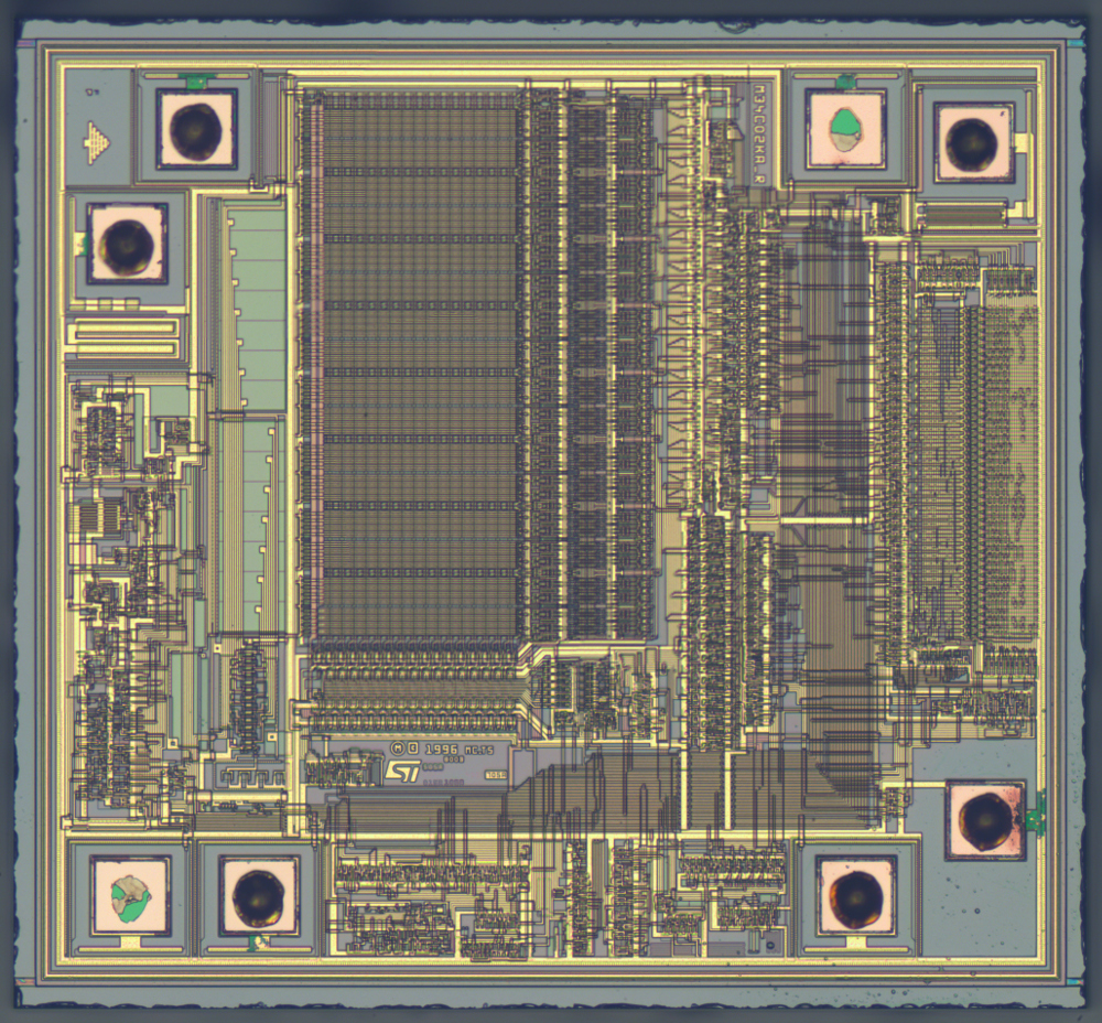
STMicroelectronics 34C02 is an 2048-bit EEPROM with hardwire write-protect and I2C interface, typically used as SPD chip in DIMM memory modules.Die size 1542x1422 µm, 1.2µm half-pitch.
January 12, 2014
Microchip 24LCS52 : weekend die-shot
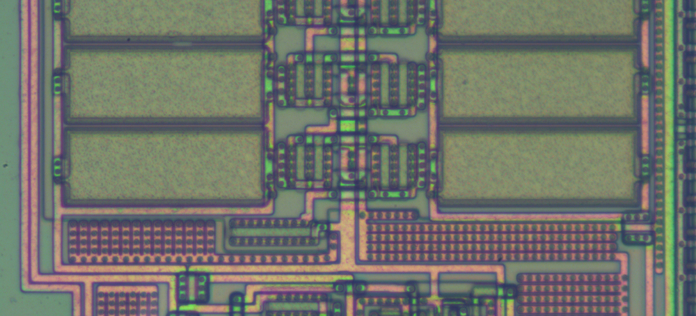
Microchip 24LCS52 is an 2048-bit EEPROM with I2C interface.Die size 1880x1880 µm, 2µm half-pitch.
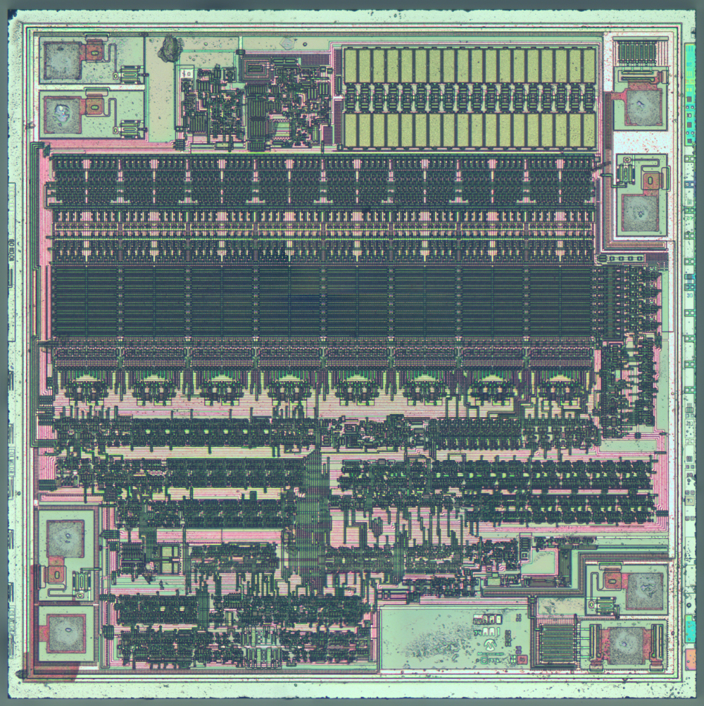
Closer look at charge-pump:
December 29, 2013
Invensense MPU6050 6-axis MEMS IMU : weekend die-shot
MEMS is probably the most requested thing we are asked about. Year ago we unsucesfully tried to take a photo of MPU6050. Now it's time for revenge!Invensense MPU6050 is an integrated gyroscope and accelerometer with 16-bit readings. It contains 2 dies, soldered/welded face-to-face in multiple places (that's what was causing us troubles last time, required temperature for separation exceeded 600C).

On the overview photo you can see how not-flat they are. On a bigger die MEMS part is 28µm above surface, on smaller die - 100 µm above. Also, there is logic right under MEMS on the bigger die.
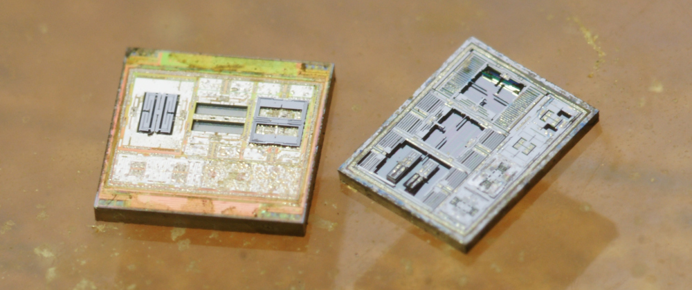
Size of big die is 2782x2718 µm, small die - 2778x2195 µm.
Read more →
December 23, 2013
1645RT2U - Milandr radhard antifuse ROM : weekend die-shot
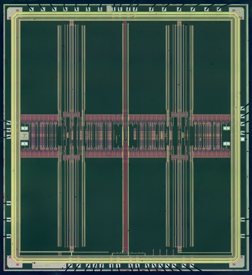
1645RT2U - radhard 32k*8 antifuse ROM, designed by Milandr. Die size - 8232x8973 µm.Minimal observed half-pitch - 680nm.
Read more →
November 4, 2013
LM2940L 1A LDO regulator : weekend die-shot
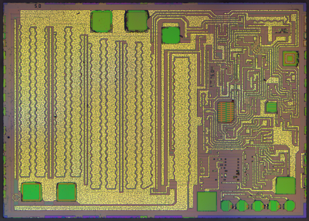
UTC LM2940L-5.0 - 1A low-dropout linear regulator.Apparently 5 contacts at the bottom-right were used to fine-tune output voltage by burning fuses between them.
October 29, 2013
KR1858VM3 - last soviet Z80 : weekend die-shot
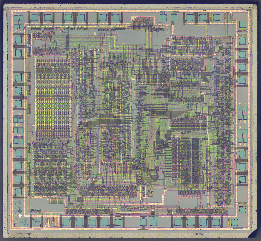
KR1858VM3 - is the lastWhile previous soviet Z80 were NMOS ones, this is 2µm CMOS. But due to "relaxed" layout (in addition to intrinsic lower logic density in CMOS) die size is even larger than 4µm NMOS variant KR1858VM1.
Die size 5050x4657 µm.
