
February 21, 2013
Part II: How to «open» microchip and what's inside? Z80, Multiclet, MSP430, PIC and more
In this article we'll continue cracking microchips open. If you've missed first article - it's here.«Canonical» way of opening microchips:
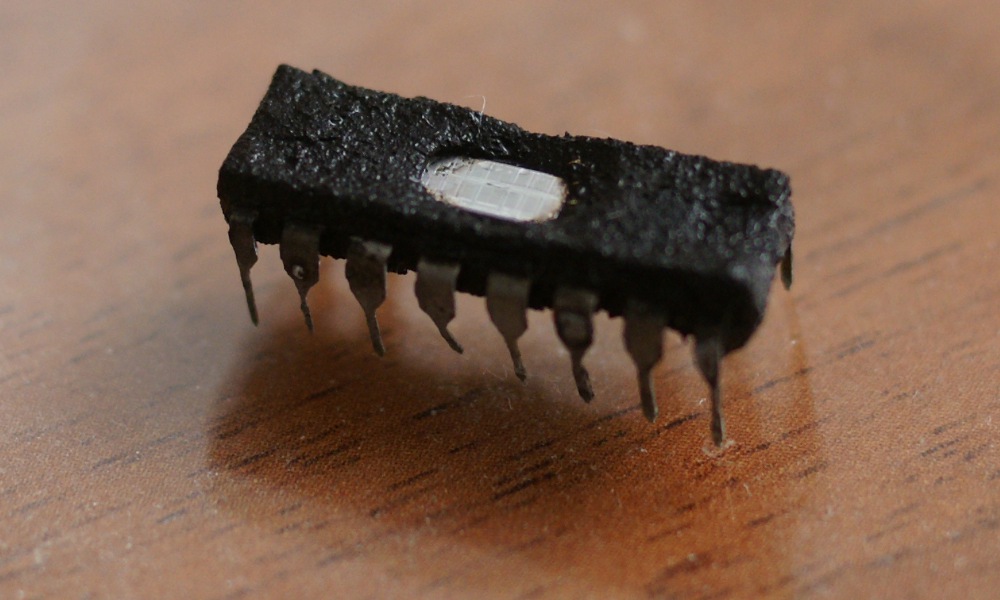
Cut a small hole in the center of the chip with a dremel: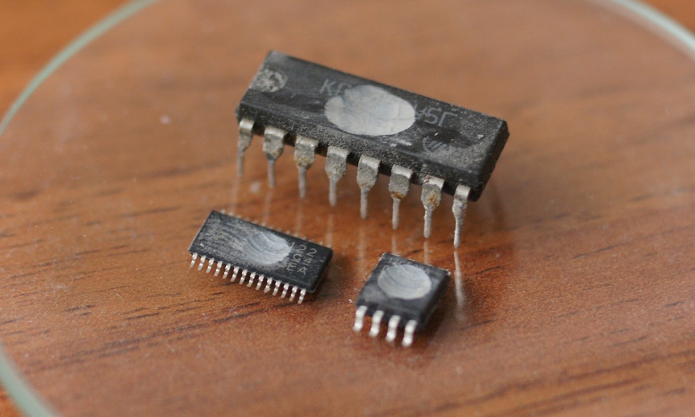
WARNING!: All operations with acids must be performed in a fume hood, with proper protection (gloves, gas mask, e.t.c).
Put a droplet of fuming nitric or sulfuric acid there, heat up to ~100 ºC (~212 ºF). It is critical to use fuming acids - just concentrated (98% sulfuric or 70% nitric) won't cut it. After reaction ends - rinse with acetone, dry and put next droplet.
As a result we are getting exposed die, with all bond wires intact. The microchip still works - this might be useful if we want to probe it or modify eeprom data with UV laser.
What's inside
K565RU5 (pin-compatible to 4164 DRAM chip) - 64 Kib DRAM chip, heart of most of amateur computers made in late soviet times and early 90's. There was also RU7 chip (256 Kib) but it was hard to buy.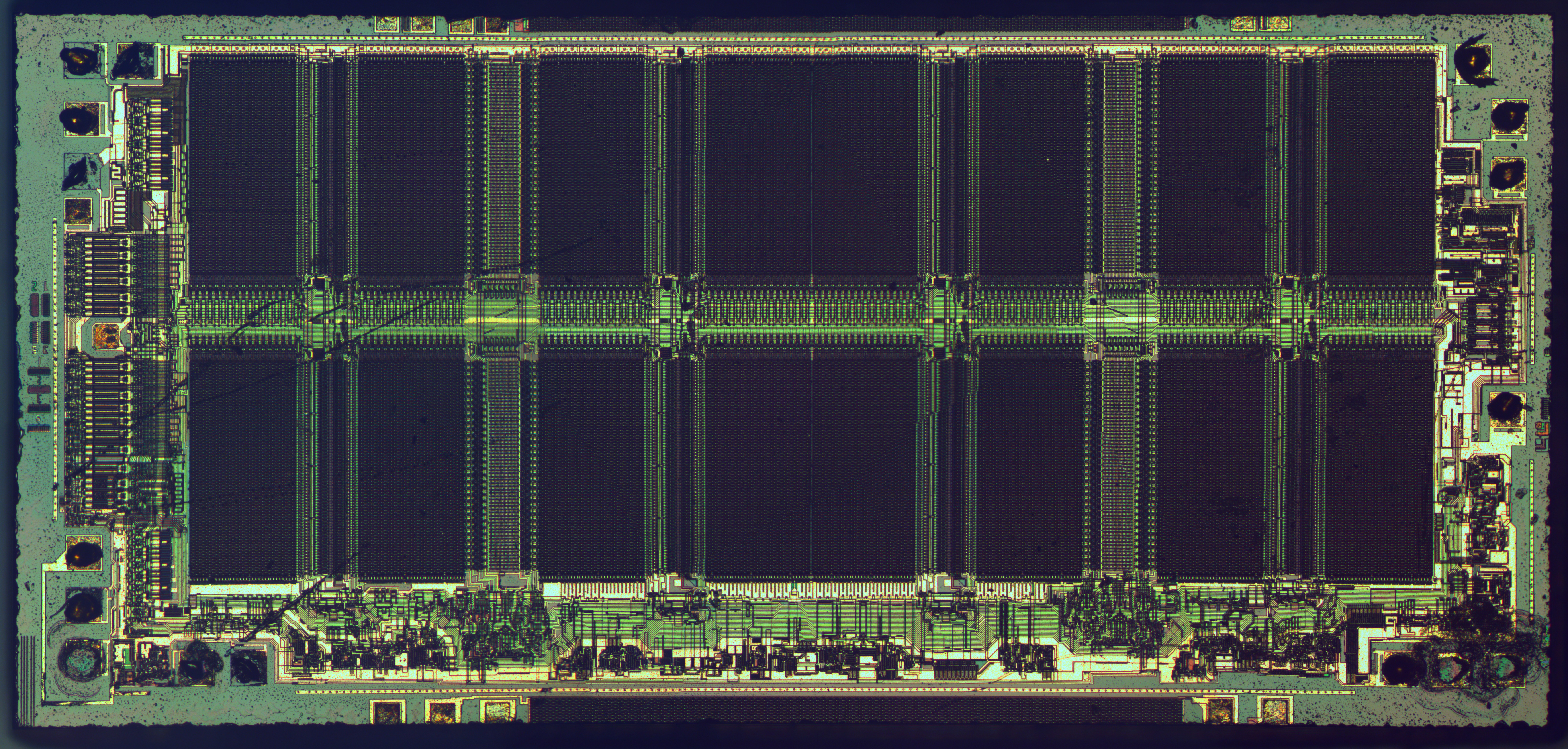
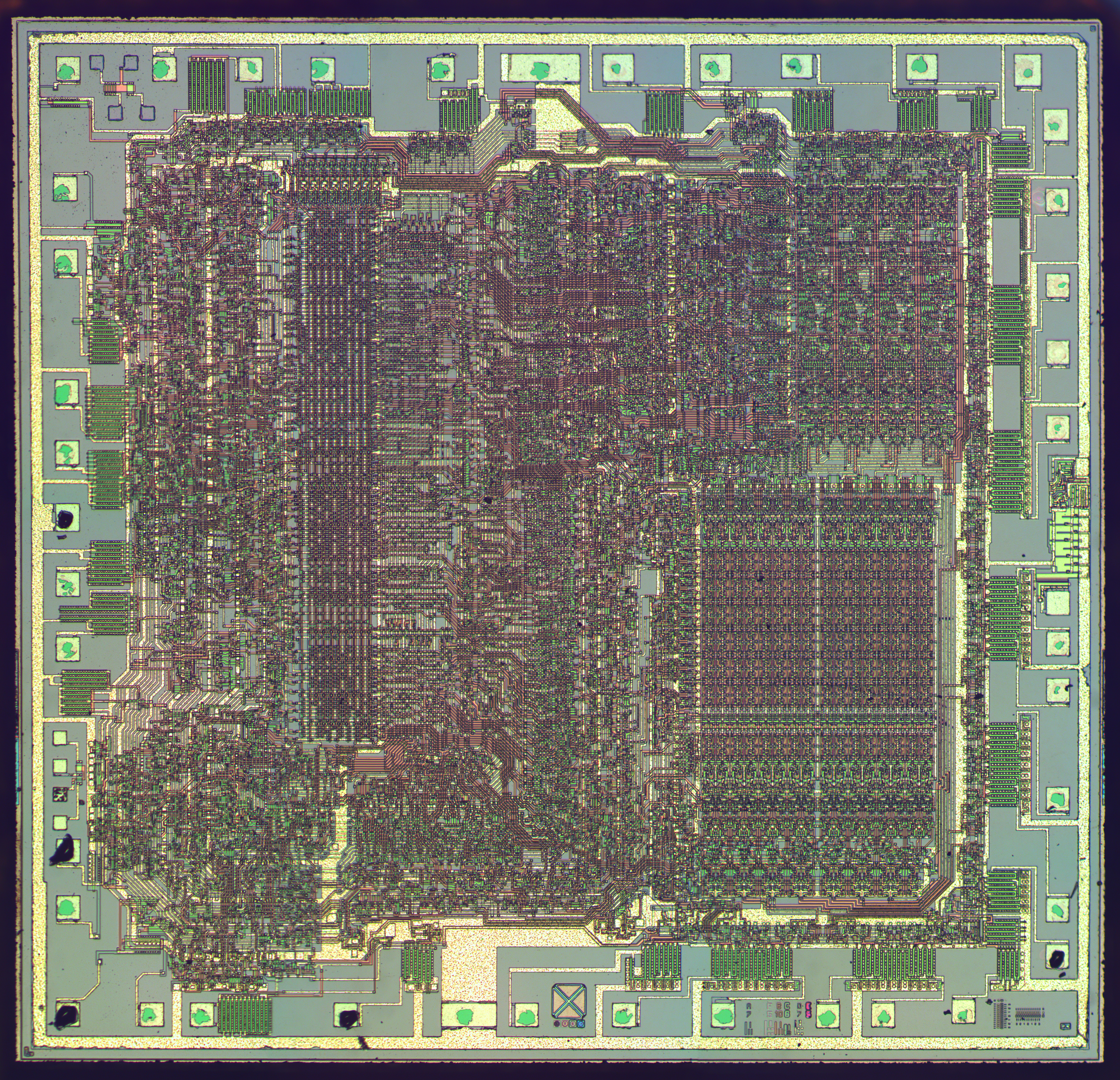
Z80A - legendary successor of Intel 8080.
This is a photo of one of it's many clones. This one is likely made in DDR by MME company.
Die size - 4950x4720 µm, technology node - 5µm.
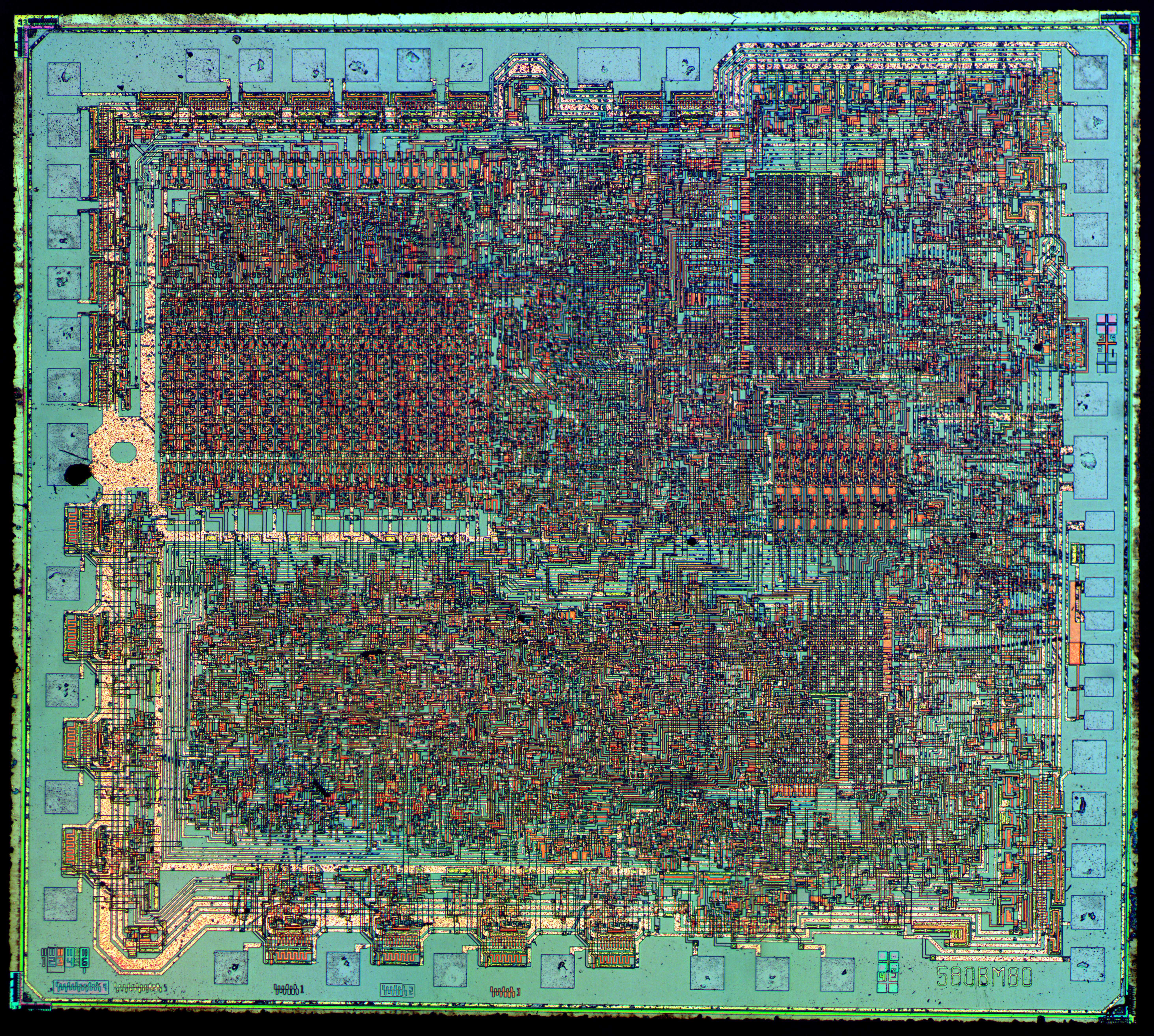
KR580VM80A just like KR580IK80A is an Intel 8080-compatible processor, which was in mass manufacturing in USSR until late 90's. Compared to KR580IK80A - die size is 20% smaller, IO peripherals are reworked.
Die size - 4634x4164 µm, 5µm technology.
MSP430F122 - 16-bit microcontroller made by Texas Instruments. What's interesting is that die is marked as MSP430F123, with larger flash size.

PIC12C508 - one of the "old" PIC's. Manufacturing technology - 1200nm, the oldest we've seen in microcontrollers being sold at the moment.
PIC16C505 - another "old" PIC, again 1200nm.

New RFID MIFARE chip from Moscow's metro - for several years Sitronics-Микрон was apparently using NXP RFID chips in Moscow's metro, but since February 2013 - we were finally able to find russian-made chips. New chip compared to NXP's one is 20% smaller, but not readable by NFC-readers in modern cell phones (might be a software issue). 180nm technology, aluminum metalization.

After metalization etch - it is clear that significant part of the chip is occupied by passive components (capacitors), and places under pads are empty.

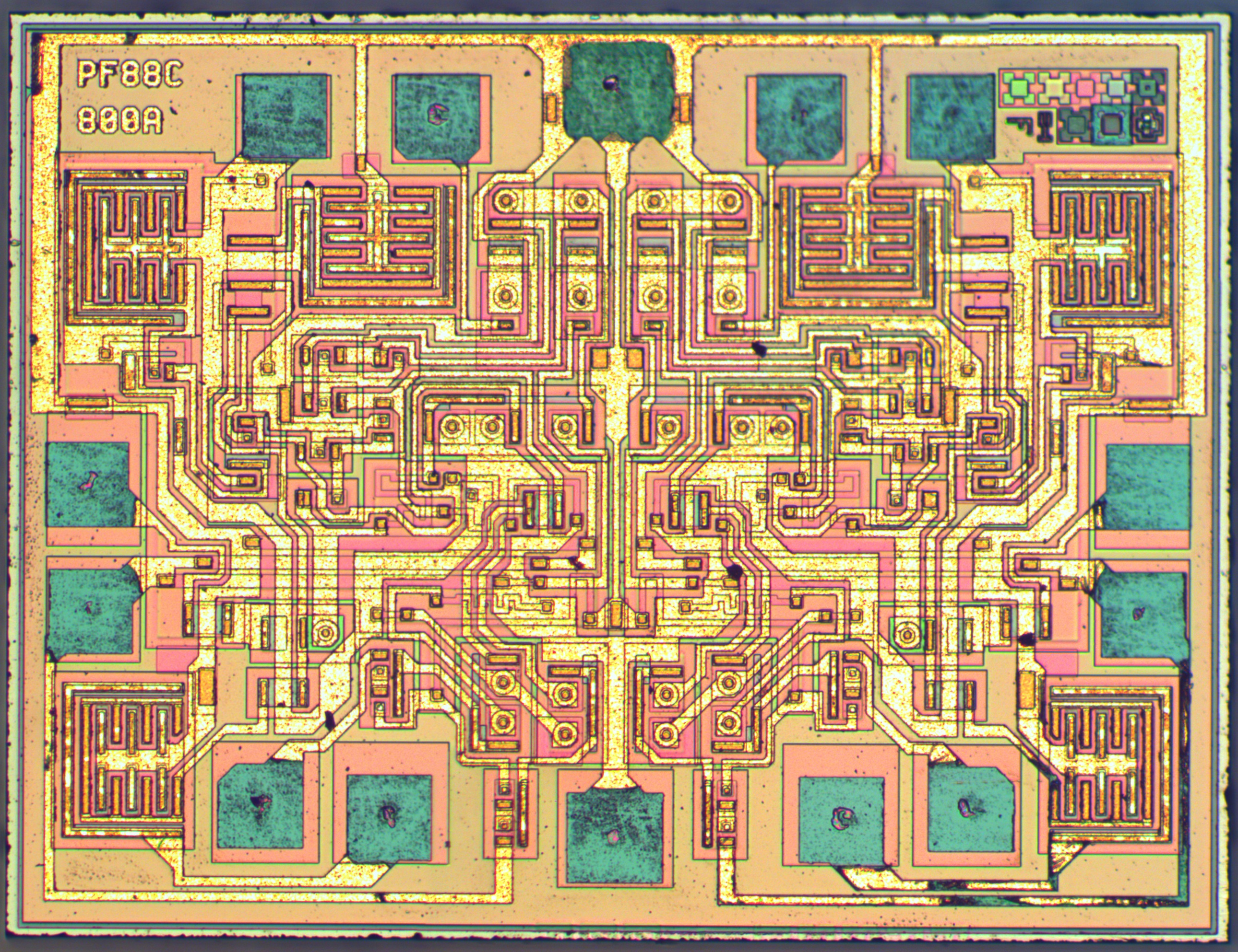
Dual timer 556 - one of the oldest chips still being manufactured.
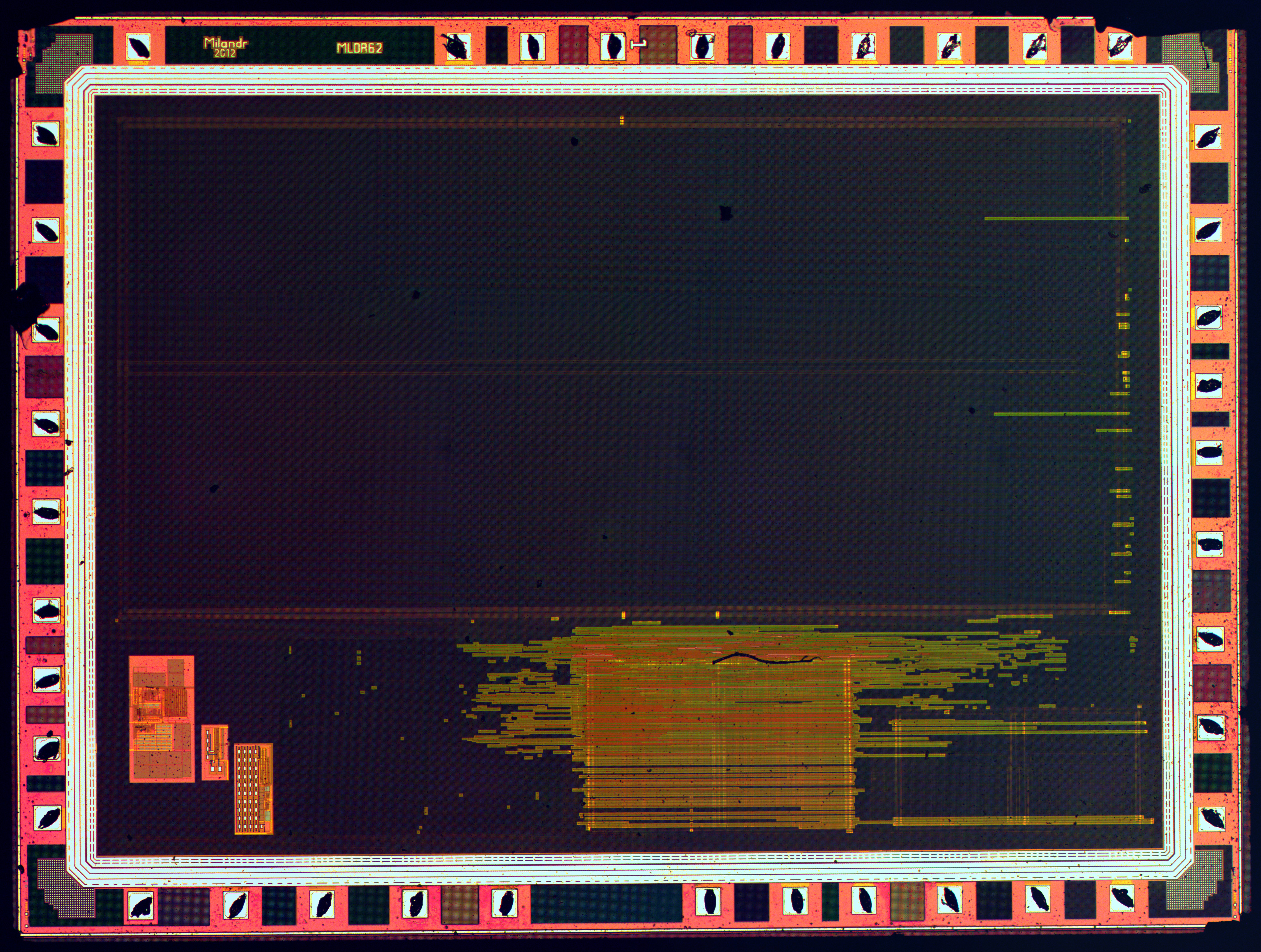
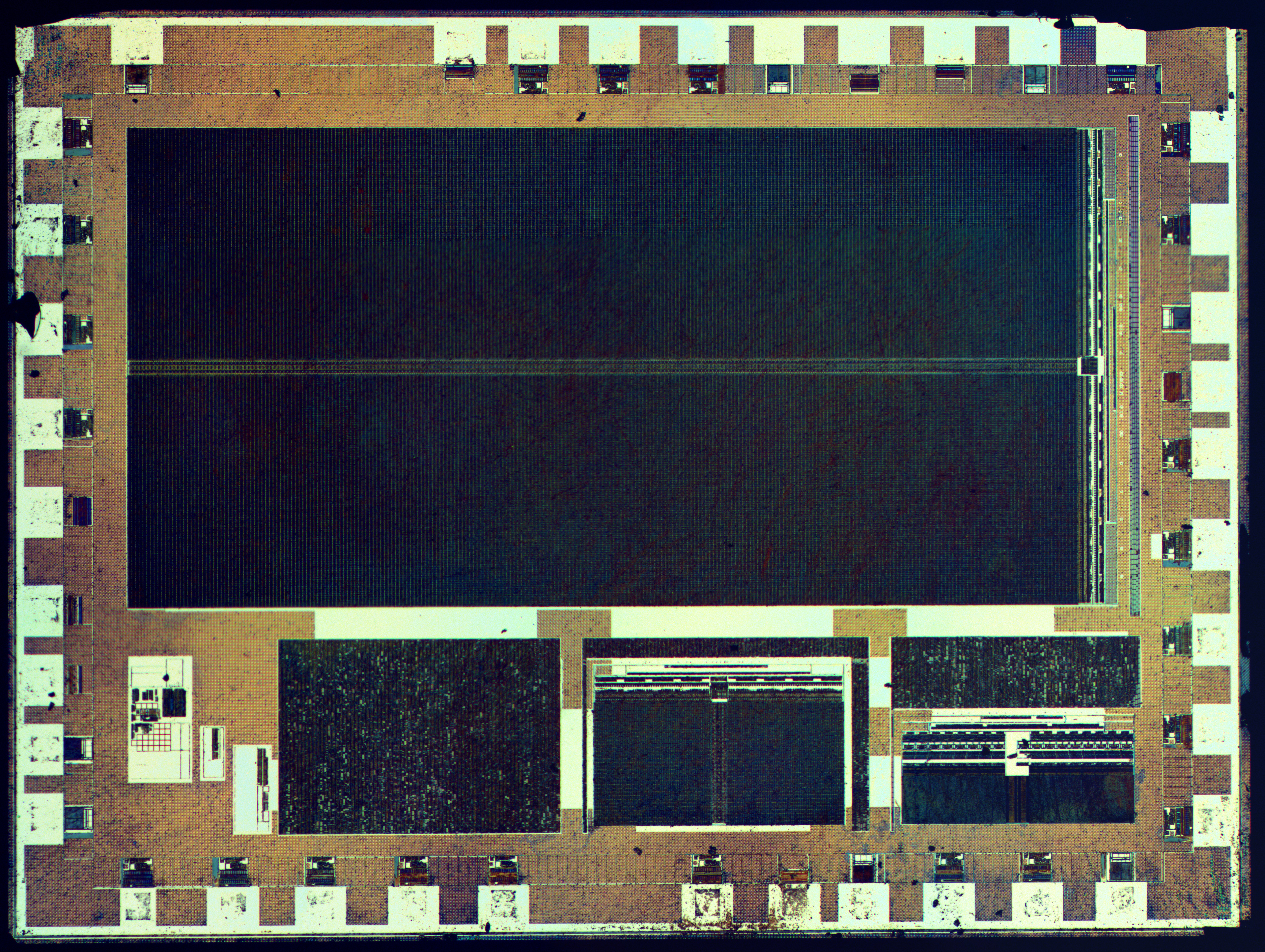
1886VE10 - Russian rad-hard 50Mhz microcontroller designed by Milandr and manufactured by Sitronics-Mikron on 180nm bulk-silicon technology. Radiation hardening is achieved by using edge-less transistors and 8T SRAM cells.
After metalization etch:
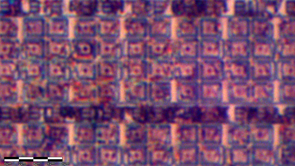
Not much to see in optical microscope:
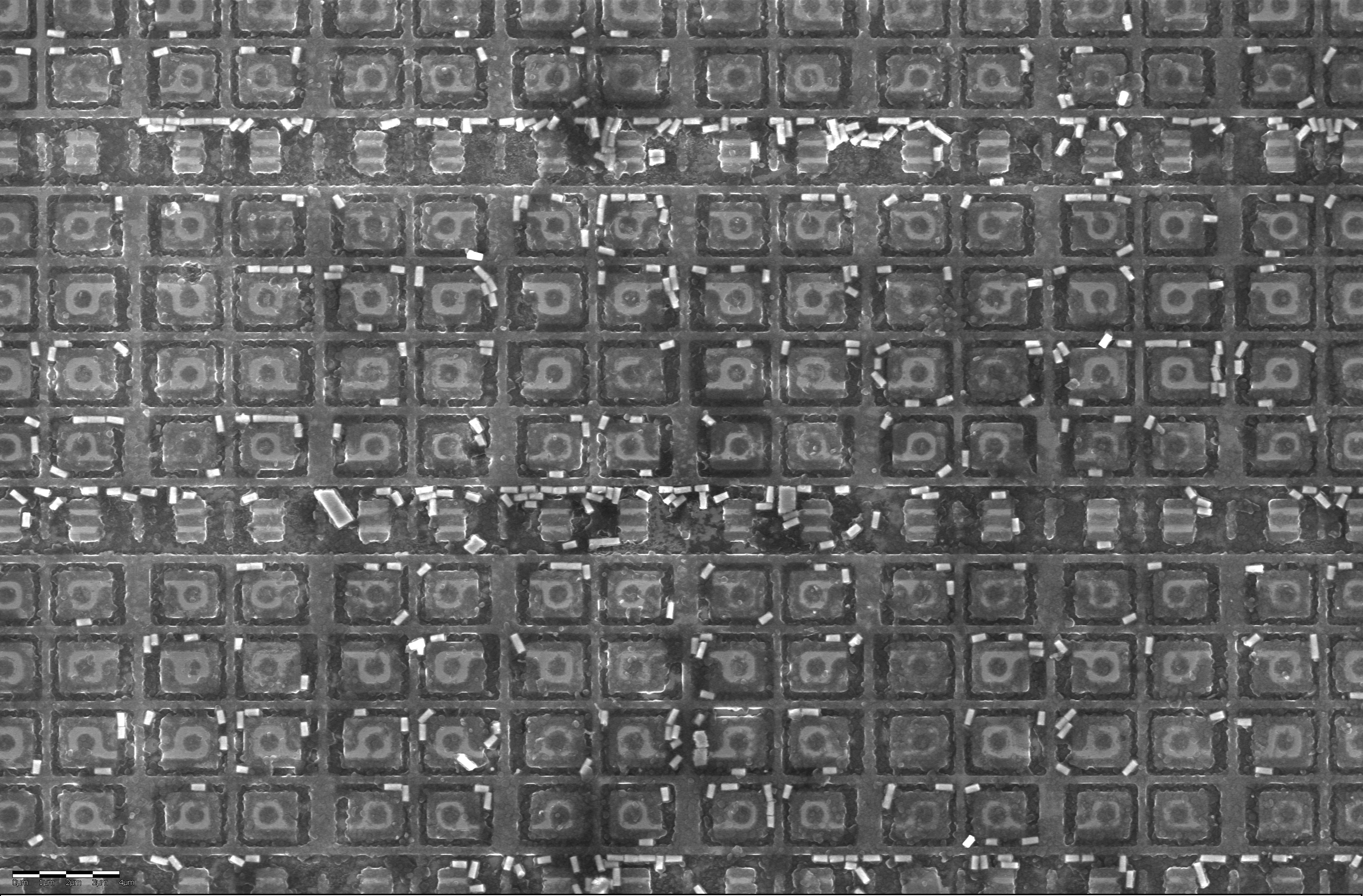
Much better via scanning electron microscope:
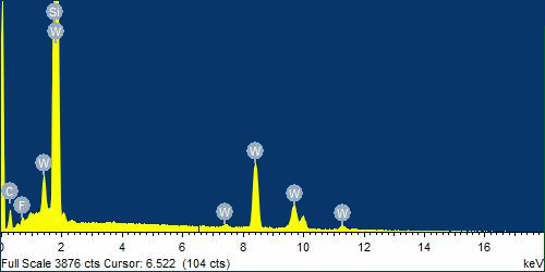
These bright cilinders - are tungsten via's left after metalization etch. This is an image from electron microprobing - sample is being bombarded by electron beam and X-Ray spectra is analyzed.
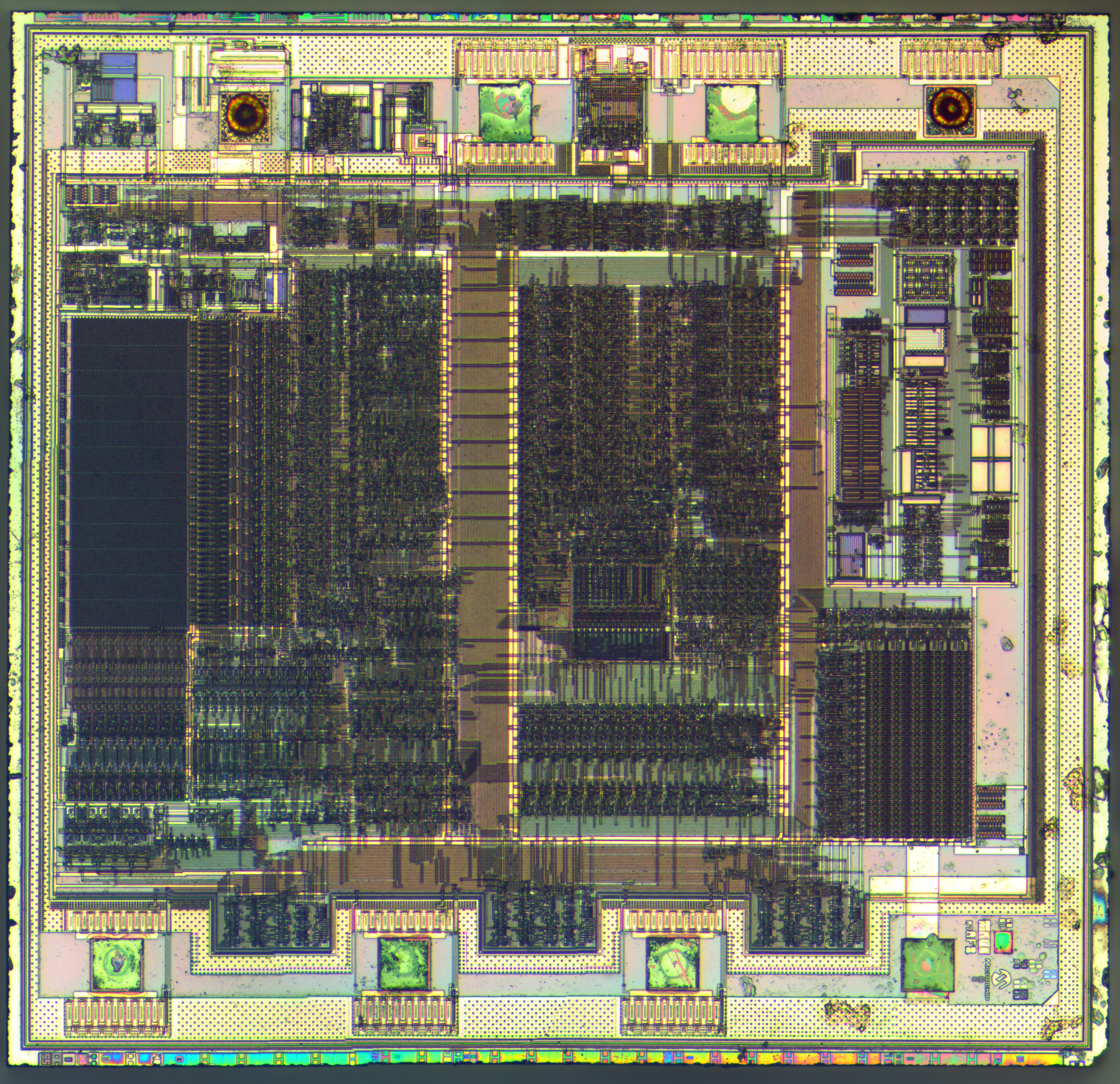
STM32 STM32F103VGT6 - one of the largest STMicroelectronics microcontrollers on Cortex-M3 core.
1Mb of flash memory and 96kb of SRAM occupies it's enormous 5339x5188 µm die.
180nm SRAM is not really visible in optical microscope:
And again, electron microscope would help us:

Multiclet MCp0411100101 - basically is a superscalar out-of-order processor(4-wide at the moment) designed in Russia. 100Mhz clock, 180nm manufacturing technology.
Die size - 10.2x10.2 мм.
After metalization etch: (Warning, high-resolution image might kill your browser)
Area of SRAM cell- 21.28 µm2. Hence, each of 16 memory blocks has 72 Kibit of RAM. Obviously, ECC codes are used(72,64). Total accessible memory is 128 KiB.
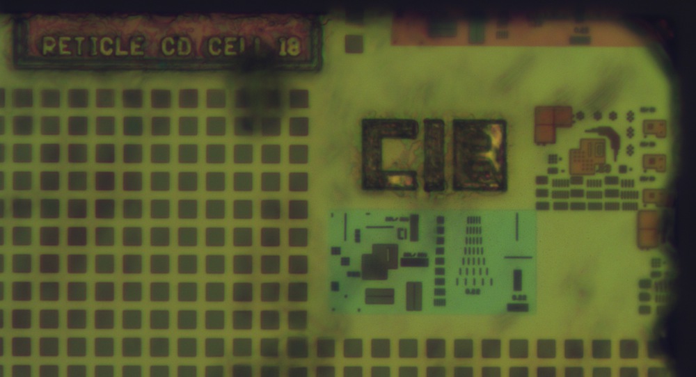
Logo's:
Also, testing areas were cut along with the crystal, for example here is critical dimension test :
Hopefully that was interesting - follow us on Twitter @Zeptobars or subscribe to our RSS feed - we'll continue opening chips.


