
February 28, 2017
A look inside Russian 28nm MIPS CPU - Baikal-T1
Many of you might have heard about Baikal-T1 - Russian implementation of dual core Imagination Technologies MIPS P5600 32 r5 with on-board 10Gb Ethernet. Baikal was the first to implement P5600 core in silicon.CPUs itself (had to go through 4 pieces to get a good die):
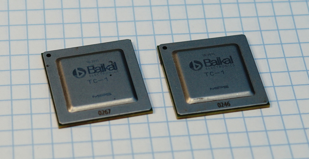
BGA-substrate and heat-spreader are similar to other modern CPUs. It's flip-chip BGA:

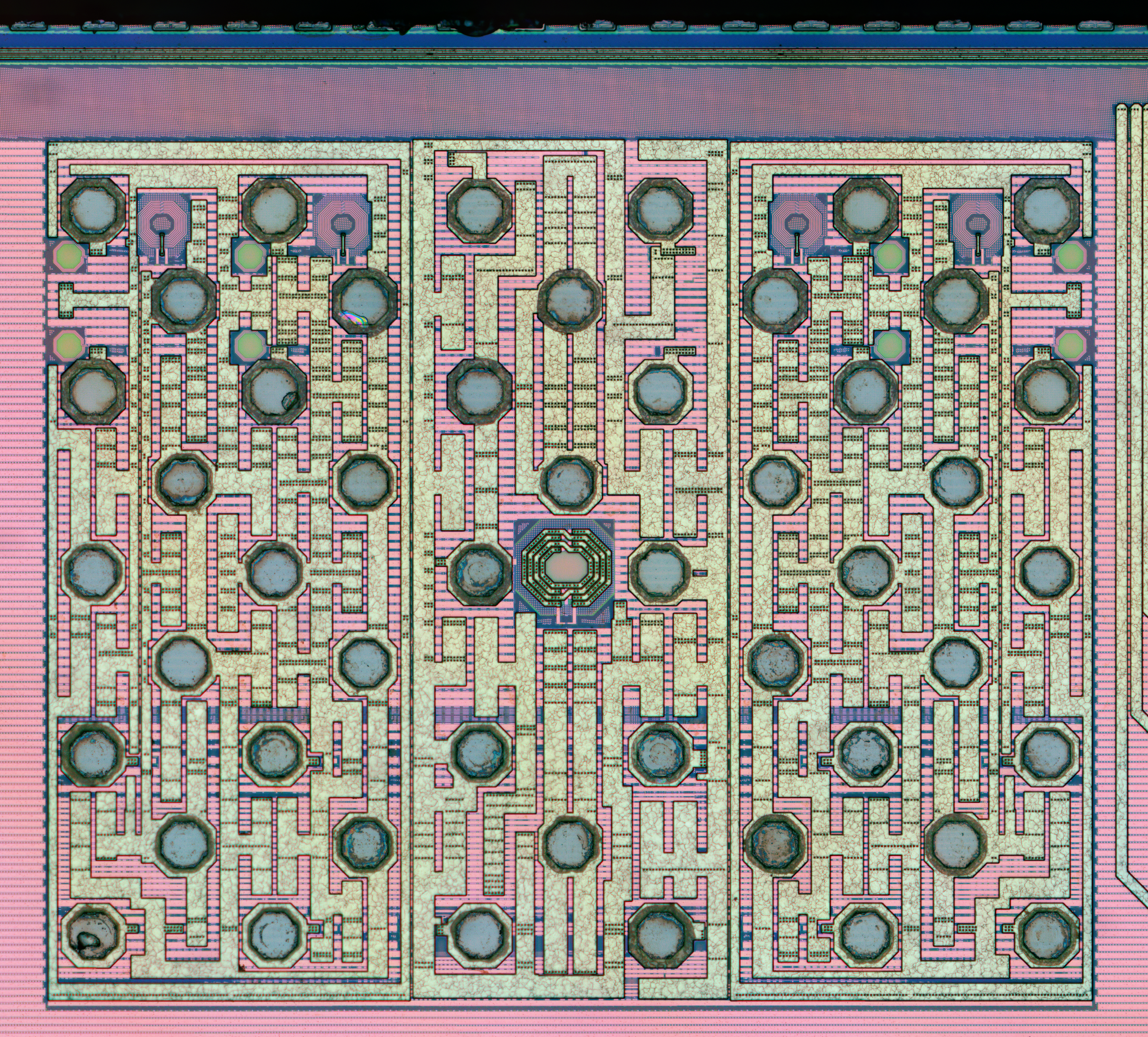
Die itself has contacts over all it's area, majority of these are VCC/GND nets. This is required not because of high power consumption (it's actually not that high, ≤5W), but rather to reduce inductance of VCC/GND nets. Again, majority of modern CPU's/SoCs use the same approach:

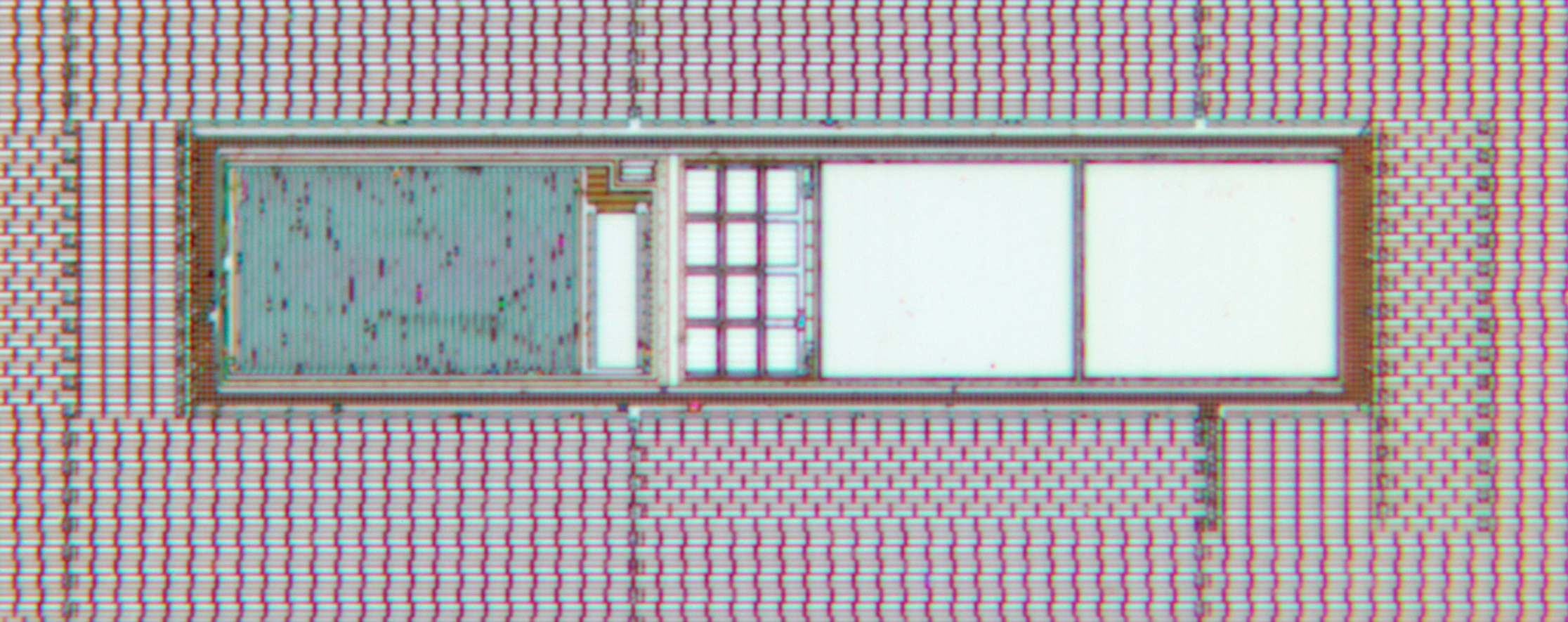
Closer look at Ethernet controller (likely 10GbE KR/KX4):
After etching metal layers - we can see auto-synthesized sea of standard cells (Multiclet CPU had similar standard cell "waves" despite significantly larger 180nm technology), lots of generated memory/register file instances (typically supplied by foundry), few supposedly monitoring blocks scattered across the area (tiny vertical blue-white rectangles). Significant part (~25%) of die area is not used by transistors, and just filled with dummy cells.

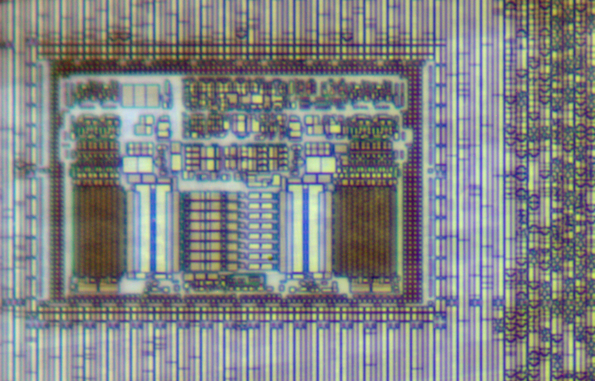
Taking a closer look: This is what I suppose a monitoring block (could measure temperature/inverter loop oscillation speed for example). Around the block - sea of dummy cells:
Columns of standard cells in highest optical resolution. 1px=28.5nm here (area on the photo has 28µm width - that's just ~0.03mm). Optical resolution is limited by diffraction to ~200nm which makes image to look quite soft. Standard cells look similar to 180nm for example - same columns of transistors back-to-back : [P N] [N P] [P N]... (i.e. neighbor columns of standard cells are mirrored). Columns with P-type transistors are slightly wider:

One of the smallest generated memory blocks. SRAM area uses only small fraction of it (the rest goes for row/column decoders, sense amplifiers and IO logic). Again, around it we can see sea of dummy cells (one cannot just leave it empty - this would cause uneven height which will ruin lithography of metal layers):
Finally - photo of Baikal CPU in immersion oil, right after last microscope shoot:

In my view Baikal-T1 is a large step forward for Russian civilian microelectronics. It uses modern commercial core, it is designed using industry-standard flow and manufactured using high-volume commercial technologies. Finally it uses open source compiler and OS - which makes it much easier to support and work with comparing to infamous Elbrus. Using non-standard solutions in situations where they could have been avoided was the curse of Russian microelectronics, until Baikal.
That's it for now. If you like articles like this one - you can now support us via Patreon or other means.


