June 11, 2013
Avalon - specialized Bitcoin processor : weekend die-shot
Yifu Guo (designer of Avalon) agreed to send us several chips for decapsulation, but while they were slowly traveling around the world - needbmw gave us damaged chip from his working Avalon mining unit.Damaged chip itself (fortunately, die itself is not damaged):
This tiny thing does 282 Mhash/s (like AMD 6970 videocard), consuming ~2.5W of power.
From public sources it is known, that chip is manufactured by TSMC at 110nm, 5 layers of metalization. One may notice that there are much more pads on the die than leads on the package - apparently many pads are connected to same leads (VCC/GND). Die size - 4.06*4.12 mm.
At the very top - we only see power distribution network:
After metalization etch we see that Avalon is large monolithic blob of logic, no any memory blocks... Square piece on the left side - is likely PLL with some control logic.
More interesting stuff visible under full magnification:
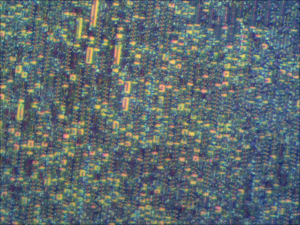
If we compare this to photo of 180nm standard-cell-based chip scaled by 61% (to match 110nm tech) we see that Avalon's logic is much denser - so I guess it is unlikely to match Avalon performance by just hitting "Synthesize" button in EDA. How it was achieved is still an open question (semi/full custom design or just TSMC's 110nm is better than we thought)