March 29, 2014
SiTime SiT8008 - MEMS oscillator : weekend die-shot
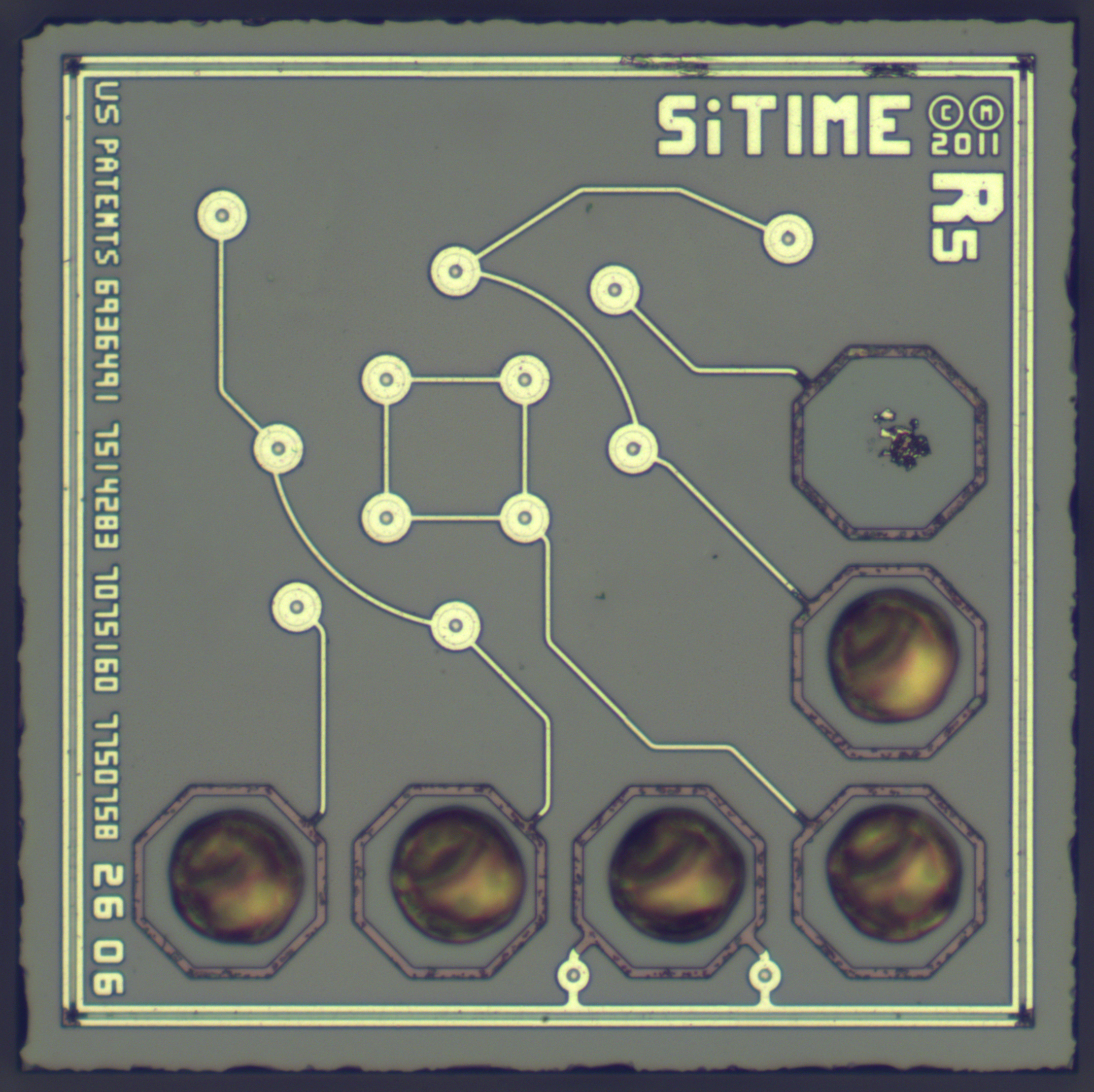
Photo of MEMS die puzzled us for quite some time. Is it some sort of integrated SAW/STW resonator?
The trick is that to reach maximum Q-factor (up to ~186'000 according to patents) MEMS resonator must operate in vacuum. So they package resonator _inside_ the die in hydrogen atmosphere, then anneal it in vacuum so that hydrogen escapes through silicon. So we see here only a cap with contacts to "buried" MEMS resonator. We were unable to reach the resonator itself without x-ray camera or ion mill.
MEMS die size - 457x454 µm.
Thankfully relevant patents were specified right on the die : US6936491 US7514283 US7075160 US7750758 :)
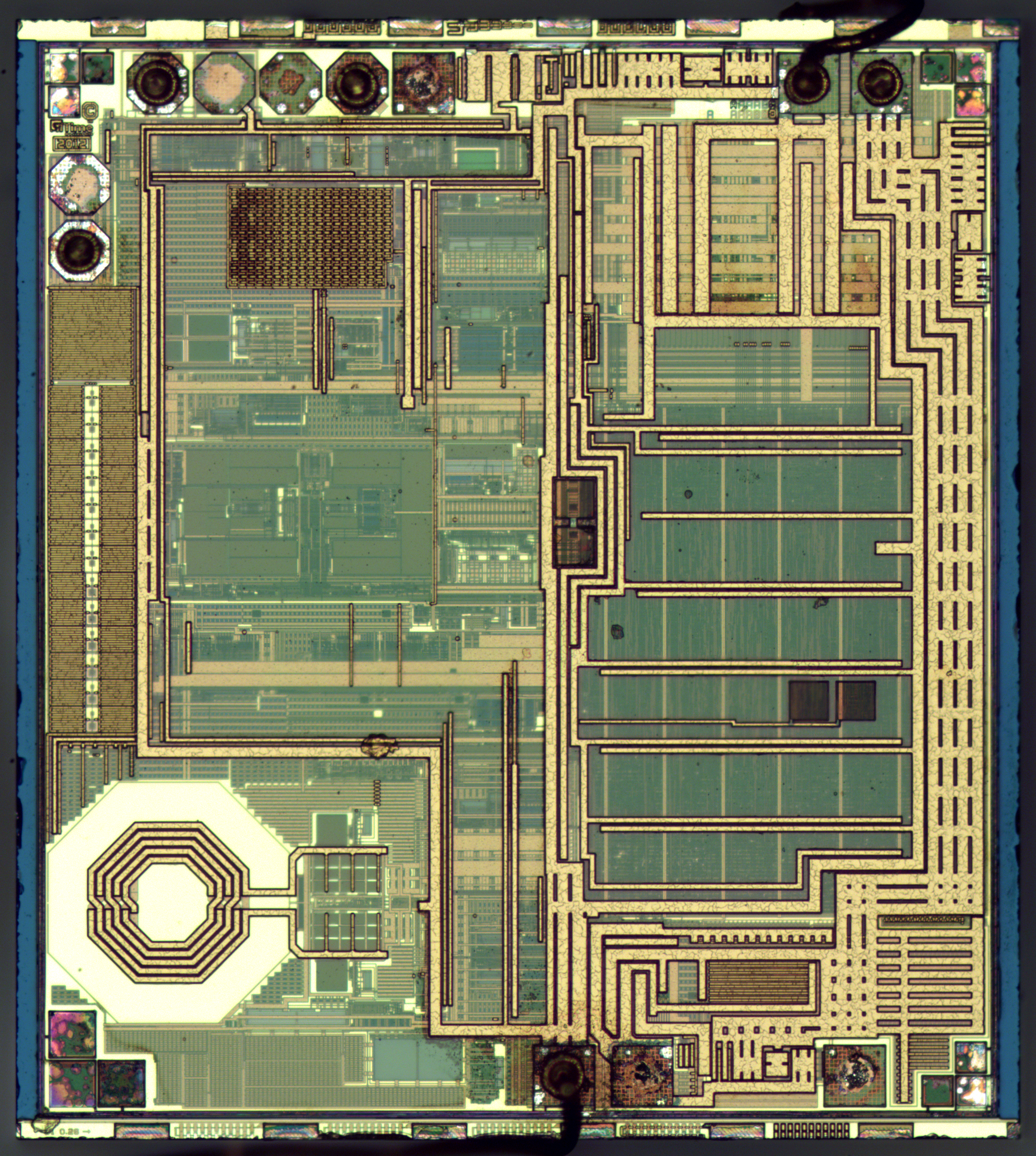
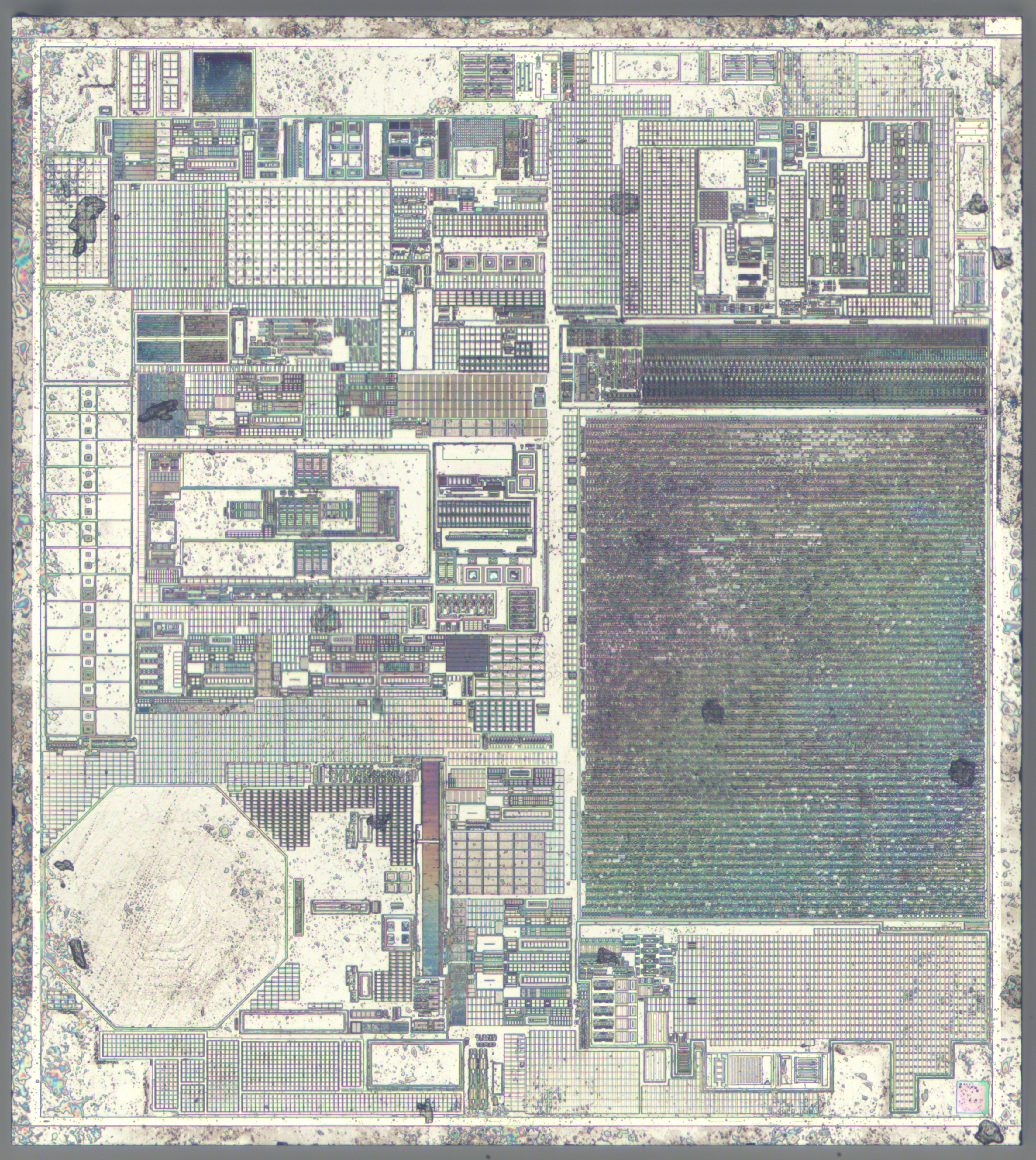
Digital die contains LC PLL and digital logic for one-off frequency programming and temperature compensation.
Die size - 1409x1572 µm.
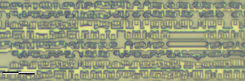
Poly level:
Standard cells ~250nm techology.