April 24, 2019
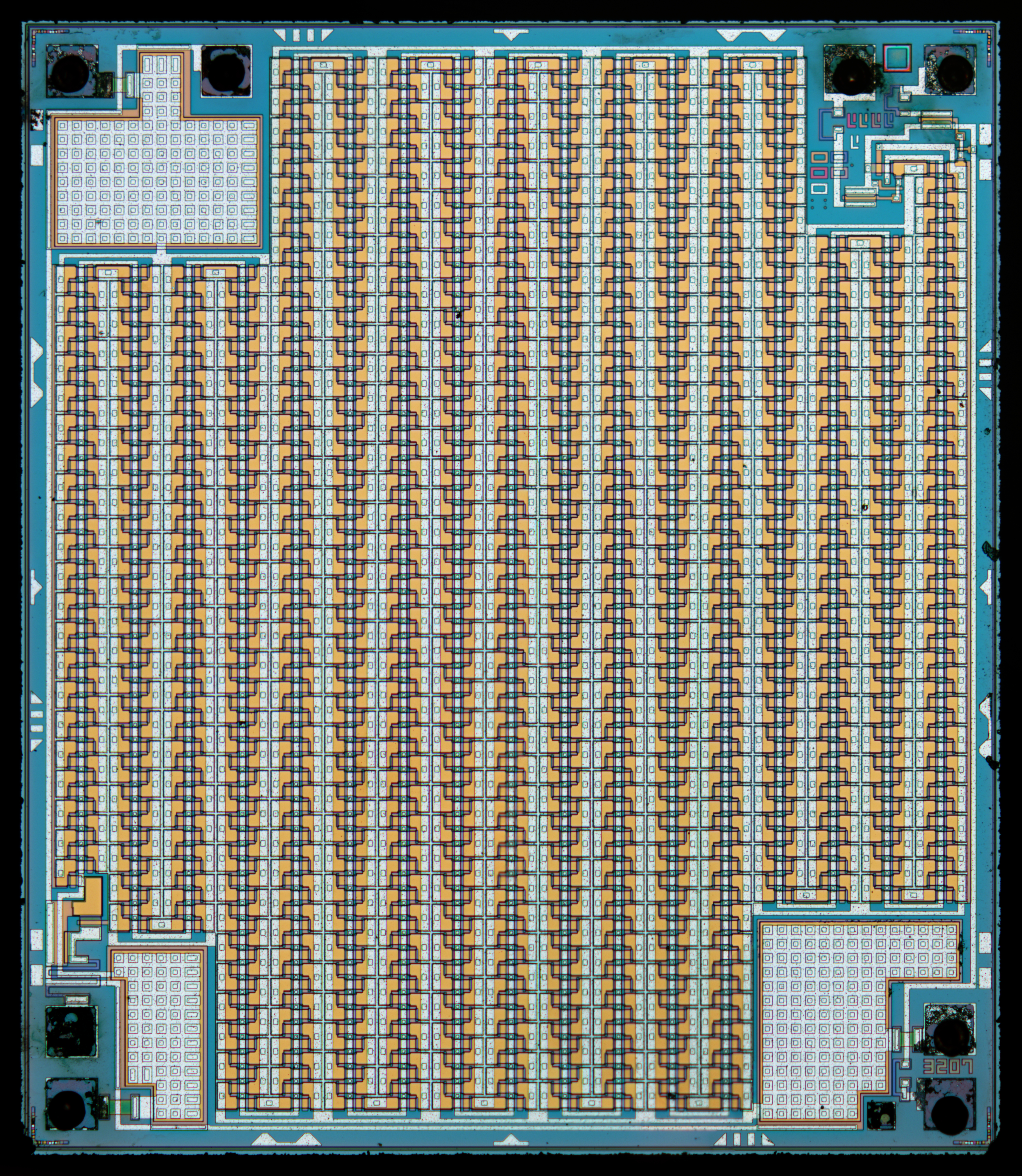
MN3207 - 1024 stage analog delay line (BBD) : weekend die-shot
MN3207 is an BBD - bucket-brigade device (predecessor of CCD) with 1024 stages used as analog delay line.Die size 2770x3210 µm.


April 13, 2019
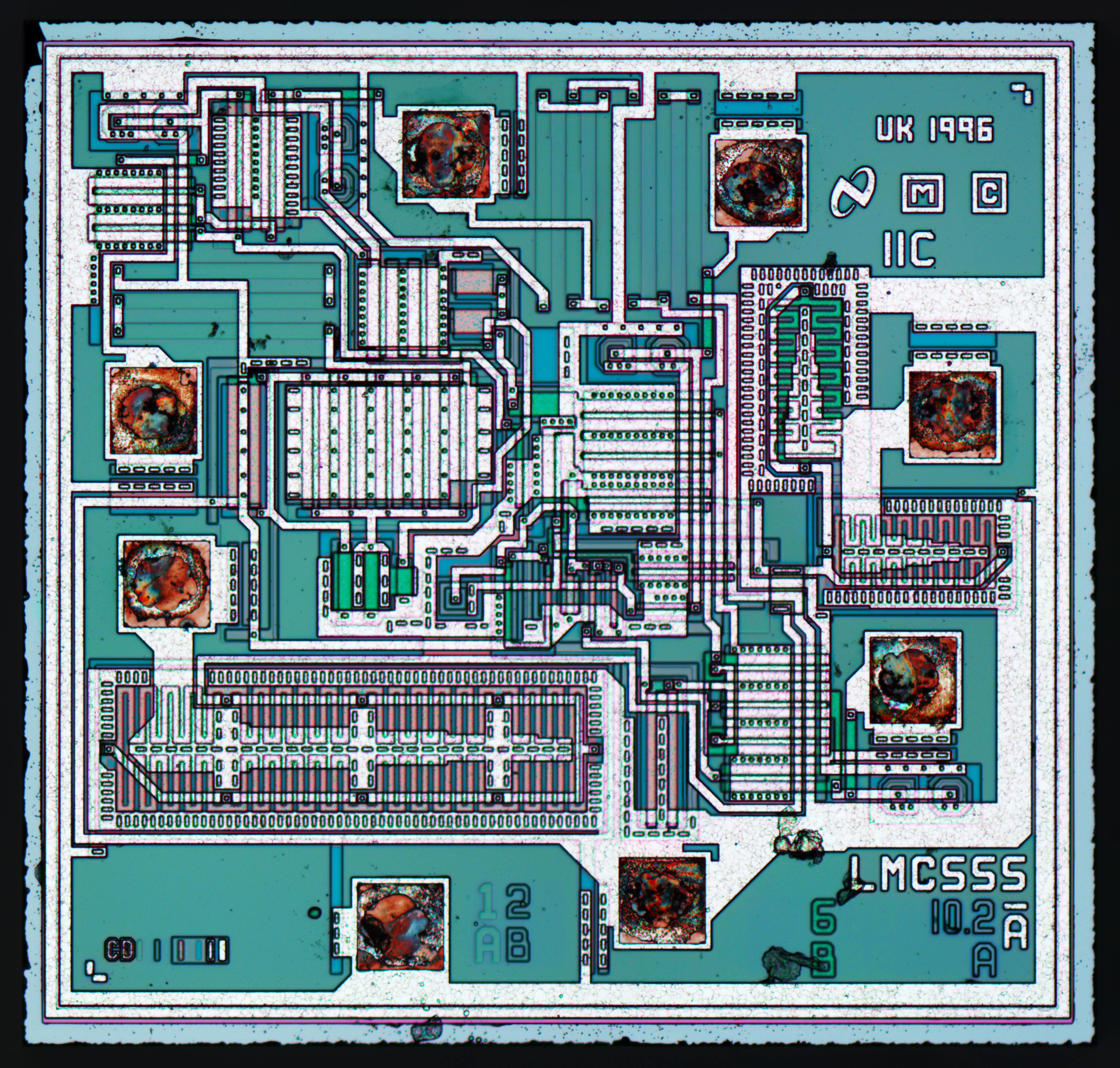
Ti LMC555CMX - CMOS 555 : weekend die-shot
This Texas Instruments LMC555CMX is almost identical to National Semiconductor LMC555.Die size 1136x1085 µm.
April 7, 2019
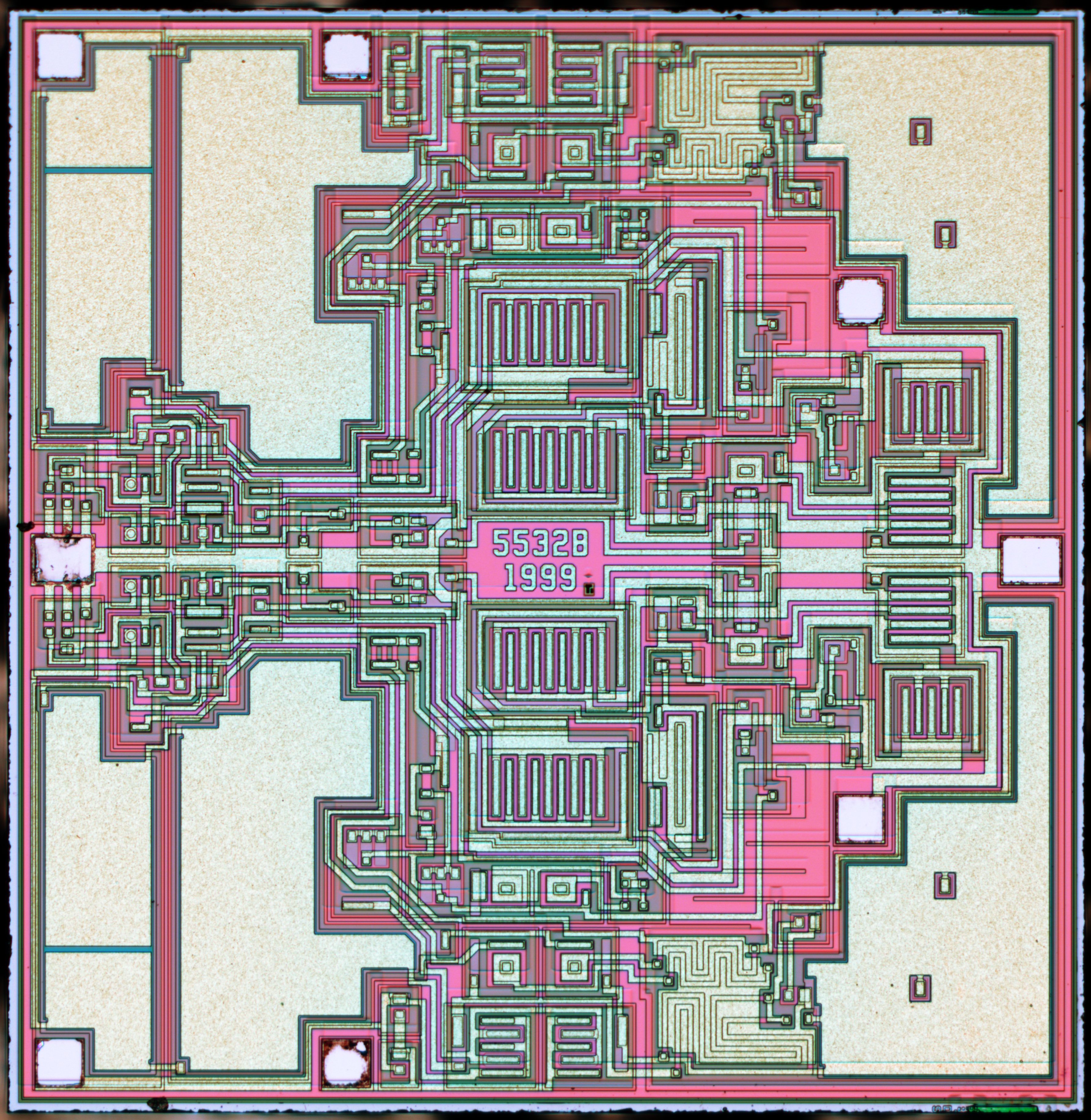
Fake audio opamp - Ti NE5532 remarked as AD OP275 : weekend die-shot
This was a weird one. After de-capping Analog Devices OP275 from audio opamp assortment kit I was surprised to see familiar Ti NE5532 die. As it was quite unusual, I de-capped original Ti NE5532 (directly from their e-shop) to confirm that older photo was indeed from genuine part, as well as one more fake OP275 to confirm that there was no mistake.It looks like someone remarked Ti NE5532 as Analog Devices OP275. Die attach and properties of plastic package also suggest Ti origin of this part.
April 6, 2019
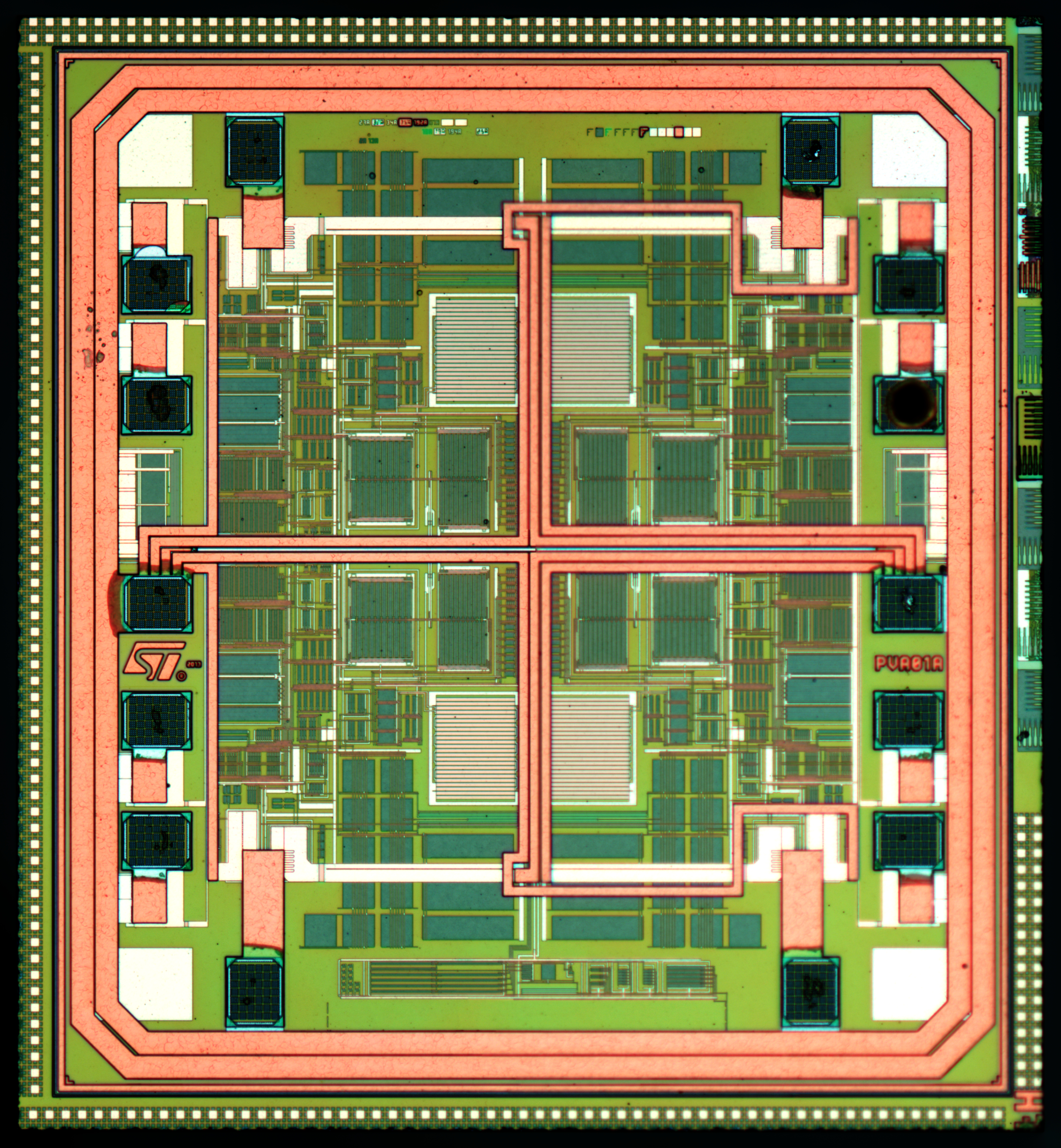
ST TSU104IPT - nanopower rail-to-rail opamp : weekend die-shot
ST TSU104IPT - is an extremely low power (580nA per channel) CMOS rail-to-rail quad opamp which could work from 1.5V source.Gain bandwidth is only 8 kHz though. Die size 1123x1219 µm.
March 8, 2019
March 8, 2019

March 1, 2019
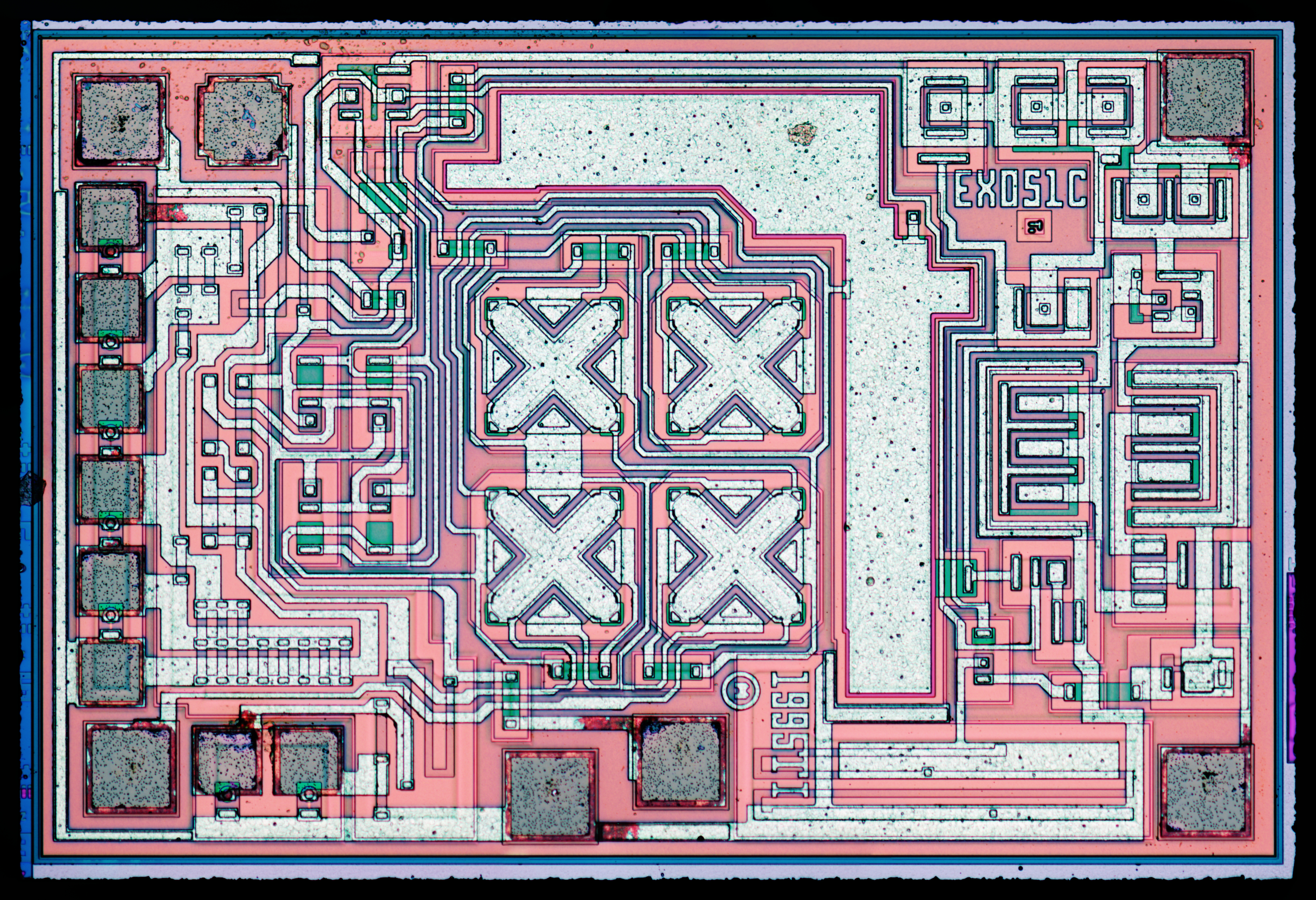
Ti TL051CDRA - trimmed JFET 20V/µs opamp : weekend die-shot
Extremely similar to BB OPA134PA.Die size 1587x1070 µm.